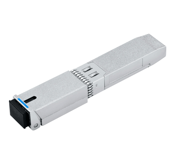

LA-GPON-ONU-34-20B-I GPON Stick ONU with Small Form-factor Pluggable (SFP) packaging, which integrates a bi-directional optical transceiver function and GPON MAC function.


LA-GPON-ONU-34-20B-I GPON Stick ONU with Small Form-factor Pluggable (SFP) packaging, which integrates a bi-directional optical transceiver function and GPON MAC function.
Regulatory Compliance
|
Feature |
Standard |
Performance |
|
Electrostatic Disge (ESD) to the Electrical Pins |
MIL-STD-883E Method 3015.7 |
Class 1 (>500V for data pins, >2000V for other pins) |
|
Electrostatic Disge (ESD) to the
Duplex LC Receptacle IEC 61000-4-2 |
IEC 61000-4-2 |
Compatible with standards |
|
Electromagnetic Interference (EMI) |
FCC Part 15 Class B
EN55022 Class B (CISPR 22B) |
Compatible with standards |
|
Immunity |
IEC 61000-4-3 |
Compatible with standards |
|
Laser Eye Safety |
FDA 21CFR 1040.10 and 1040.11
EN60950, EN (IEC) 60825-1, 2 |
Compatible with Class I laser product |
|
RoHS |
2011/65/EC |
Compliant with standards |
Absolute Maximum Ratings
It has to be noted that the operation in of any individual absolute maximum ratings might cause permanent damage to this module.
|
Parameter |
Symbol |
Min |
Typ. |
Max |
Unit |
Notes |
|
Operating Voltage |
Vcc |
3.14 |
3.3 |
3.6 |
V |
|
|
Storage Temperature |
Ts |
-40 |
|
85 |
℃ |
|
|
Operating Relative Humidity |
RH |
15 |
|
85 |
% |
1 |
Notes:
1. Non-condensing
Recommended Operating Environment
Electrical and optical acteristics below are defined under this operating environment, un- less otherwise specified
|
Parameter |
Symbol |
Min |
Typ. |
Max |
Unit |
Notes |
|
Operating Case Temperature |
Top |
-40 |
|
85 |
℃ |
|
|
Total Tx and Rx Supply Current |
ICC |
|
600 |
|
mA |
|
|
Power Dissipation |
PD |
|
2
|
|
W |
|
|
Bit Rate (Tx) |
BR |
|
1244.16 |
|
|
|
|
Bit Rate (Rx) |
BR |
|
2488.32 |
|
|
|
|
Transmission Distance |
TD |
|
|
20 |
km |
|
|
Module Initialize time |
T_Initial |
|
|
70 |
S |
1 |
|
Two-wire serial interface Clock rate |
f_serial_clock |
|
|
80 |
Khz |
|
Notes:
1. Suggest do not access I2C until module initialization is complete
Electrical Characteristics
|
Parameter |
Symbol |
Min |
Typ. |
Max |
Unit |
Notes |
|
Transmitter |
||||||
|
Differential Data Input Voltage |
VIN, P-P |
100 |
|
1000 |
mVpp |
1 |
|
Input Differential Impedance |
ZIN |
|
100 |
|
Ω |
2 |
|
Receiver |
||||||
|
Differential Output Voltage |
|
370 |
|
1000 |
mV |
3 |
|
Signal Detect Output HIGH Voltage |
VSD_High |
2.4 |
|
|
V |
4 |
|
Signal Detect Output LOW Voltage |
VSD_Low |
0 |
|
0.8 |
V |
5 |
|
Data Output Rise and Fall Time |
TR/TF |
|
160 |
|
PS |
|
Notes:
1. TXD+/-. AC-coupled.
2. TXD+/-.
3. CML output, AC coupled(0.1mF)
4. LVTTL with internal 1kW pull up resistor. Asserts HIGH when input data amplitude is above threshold.
5. LVTTL. De-asserts LOW when input data amplitude is below threshold.
Optical Characteristics
|
Parameter |
Symbol |
Min |
Typ. |
Max |
Unit |
Notes |
|
Transmitter |
||||||
|
Center Wavelength Range |
λC |
1290 |
1310 |
1330 |
mm |
1 |
|
Average Output Power |
P0UT |
0.5 |
|
5 |
dBm |
|
|
Average Output Power (Laser Off) |
P0UT-OFF |
|
|
-40 |
dBm |
|
|
Side Mode Suppression Ratio |
SMSR |
30 |
|
|
dB |
|
|
Spectral Width (-20dB) |
λ20 |
|
|
1 |
nm |
|
|
Extinction Ratio |
ER |
10 |
|
|
dB |
1 |
|
Optical Rise and Fall Time (20%-80%) |
TR/TF |
|
|
250 |
ps |
|
|
Jitter Generation |
JG |
|
|
250 |
ps |
|
|
Transmitter Output E |
Compliant with G.984.2 Figure 3 |
|||||
|
Receiver |
||||||
|
Center Wavelength Range |
λC |
1480 |
1490 |
1500 |
mm |
|
|
Overload |
|
-8 |
|
|
dBm |
|
|
Sensitivity (BOL Room Temp) |
Sen |
-28 |
|
|
dBm |
3 |
|
Signal Detect Assertion Level |
SDA |
|
|
-29 |
dBm |
|
|
Signal Detect De-Assertion Level |
SDD |
-45 |
|
|
dBm |
|
|
Hysteresis |
PSDA-SDD |
0.5 |
|
6 |
dB |
|
|
1310nm Tx to 1490nm Rx Crosstalk |
|
|
|
-47 |
dB |
|
|
1555nm Rx to 1490nm Isolation |
|
30 |
|
|
dB |
|
|
(1550-1560nm) Ext to 1490 Rx Isolation |
|
34 |
|
|
dB |
|
|
Back Reflection @ 1310nm |
|
|
|
-12 |
dB |
|
|
Back Reflection @ 1490nm |
|
|
|
-27 |
dB |
|
|
Rx Reflectance |
|
|
|
-20 |
dB |
|
|
1530nm to 1490nm Rx Isolation |
|
7 |
|
|
dB |
|
|
1539nm to 1490nm Rx Isolation |
|
22 |
|
|
dB |
|
|
1625nm to 1490nm Rx Isolation |
|
22 |
|
|
dB |
|
|
1310nm Tx to 1490nm Rx Crosstalk |
|
- |
- |
-47 |
dB |
|
|
1555nm Rx to 1490nm Isolation |
|
30 |
- |
- |
dB |
|
Notes:
1.Measured by Ethernet package with random payload.
2. 4kHz to 10MHz
3. Measured with Ethernet package with random payload and ER=8.2dB, BER =10-10.
Pin Definitions
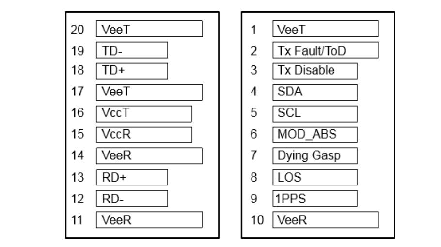
|
Pin |
Symbol |
Logic |
Description |
Notes |
|
1 |
VeeT |
NA |
Module Transmitter Ground |
3.6 |
|
2 |
Tx Fault/ToD |
LVTTL-OT |
Tx Fault/Time of Day |
85 |
|
3 |
TX_DISABLE |
LVTTL-I |
Transmitter Shut-off |
6 |
|
4 |
SDA |
LVTTL-I/O |
2-Wire Serial Interface Data Line (MOD-DEF2) |
2, 7 |
|
5 |
SCL |
LVTTL-I |
2-Wire Serial Interface Clock (MOD-DEF1) |
2, 7 |
|
6 |
MOD_ABS |
NA |
Module Absent, connected to VeeT or VeeR in the module |
|
|
7 |
DYING GASP |
Analog Input |
Dying Gasp message indicator, active low
this pin has been directly connected to MAC IC in the module |
3, 4, 5, 7 |
|
8 |
LOS |
LVTTL-O |
Loss of Signal |
|
|
9 |
1PPS |
LVTTL-O |
1 Pulse per second |
|
|
10 |
VeeR |
NA |
Module Receiver Ground |
|
|
11 |
VeeR |
NA |
Module Receiver Ground |
|
|
12 |
RXD- |
CML-O |
Receiver Inverted Data Output |
|
|
13 |
RXD+ |
CML-O |
Receiver Non-Inverted Data Output |
|
|
14 |
VeeR |
NA |
Module Receiver Ground |
|
|
15 |
VCCR |
NA |
Module Receiver 3.3V Supply |
|
|
16 |
VCCT |
NA |
Module Transmitter 3.3V Suppl |
|
|
17 |
VeeT |
NA |
Module Transmitter Ground |
|
|
18 |
TXD+ |
CML- |
Transmitter Non-Inverted Data Input, CML, 100ohm
differential impedance |
|
|
19 |
TXD- |
CML-I |
Transmitter Inverted Data Input, CML, 100ohm differential
impedance |
|
|
20 |
VeeT |
NA |
Module Transmitter Ground |
|
Notes:
1. Default Factory Mode is Tx Fault. For Small Celll type of applications, during Activation/ provisioning, it will be software configured to ToD.
2. This PIN is an open collector/drain output pin and shall be pulled up with 4.7K-10K ohms to a Host_Vcc on the host board.
3. IN7 can support Dying Gasp function. Dying Gasp function is managed by software. If software disables the dying gasp function, ignore the PIN7 input voltage. If software enables the function, PIN7 input voltage below Dying Gasp Assert Voltage threshold, the module will report dying gasp PLOAM to OLT.
4. Dying Gasp Voltage threshold 1.5V ( typical), once software enable Dying gasp, meanwhile the pin7 input is below this threshold, it will trigger dying gasp function, transceiver will reset.
5. Host device shall maintain power to ONU module for at least 10ms during power supply drop.
6. ONU re-online process includes downlink & uplink synonization, authentication and configuration release, etc., it normally takes >=5 seconds
7. Transceiver full power on need 80s. Any I2C visiting.etc need to operate after this power on period.
EPROM Information
EEPROM Diagram
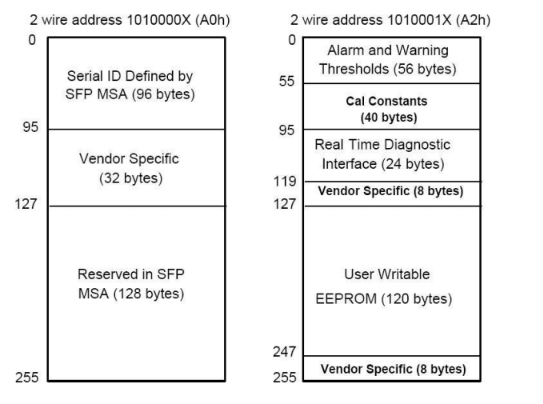
EEPROM Memory Content (A0h)
|
Addr. |
Field Size (Bytes) |
Name of Field |
Hex |
Description |
|
0 |
1 |
Identifier |
03 |
SFP transceiver |
|
1 |
1 |
Ext. Identifier |
04 |
MOD4 |
|
2 |
1 |
Connector |
01 |
SC |
|
3-10 |
8 |
Transceiver |
00 00 00 00 00 00 00 00 |
2, 7 |
|
11 |
1 |
Encoding |
03 |
NRZ |
|
12 |
1 |
BR, Nominal |
0C |
1.244Gbps |
|
13 |
1 |
Reserved |
00 |
3, 4, 5, 7 |
|
14 |
1 |
Length (9um)-km |
14 |
20(km) |
|
15 |
1 |
Length (9um) |
C8 |
200(100m) |
|
16 |
1 |
Length (50um) |
00 |
Not Support MMF |
|
17 |
1 |
Length (62.5um) |
00 |
Not Support MMF |
|
18 |
1 |
Length (Copper) |
00 |
Not Support Copper |
|
19 |
1 |
Reserved |
00 |
|
|
20-35 |
16 |
Vendor name |
53 4F 55 52 43 45 50 48
4F 54 4F 4E 49 43 53 20 |
“FS “(ASCII) |
|
36 |
1 |
Reserved |
00 |
|
|
37-39 |
3 |
Vendor OUI |
00 00 00 |
|
|
40-55 |
16 |
Vendor PN |
53 50 53 33 34 32 34 54
48 50 54/45 44 46 50 20 20 |
“GPON-ONU-34-20BI”(ASCII) |
|
56-59 |
4 |
Vendor Rev |
xx xx 20 20 |
ASCII(“30 31 20 20” means 1.0 Revision) |
|
60-61 |
2 |
Wavelength |
05 1E |
Tx wavelength: 1310nm |
|
62 |
1 |
Reserved |
00 |
|
|
63 |
1 |
CC_BASE |
xx |
Check sum of byte 0-62
|
|
64-65 |
2 |
Options |
00 1A |
64 = 0x00, reserved
65 = 0x1A, TX_DISABLE/
TX_FAULT/RX_LOS supported |
|
66 |
1 |
BR, max |
00 |
|
|
67 |
1 |
BR, max |
00 |
|
|
68-83 |
16 |
Vendor SN |
xx xx xx xx xx xx xx xx
xx xx xx xx xx xx xx xx |
ASCII |
|
84-91 |
8 |
Date code |
xx xx xx xx xx xx 20 20 |
Year(2 bytes),Month(2 bytes), Day(2
bytes) |
|
92 |
1 |
Diagnostic Monitoring Type |
68 |
Compliant with SFF-8472 V10.3
Internally Calibrated
Received power measurement type
-Average Power |
|
93 |
1 |
93 |
F0 |
Diagnostics
(Optional Alarm/warning flags)
Soft TX_FAULT monitoring
implemented.
Soft RX_LOS monitoring
implemented |
|
94 |
1 |
SFF-8472 Compliance |
05 |
Indicates the revision of SFF-8472 with which the transceiver complies. Value depends on module features. |
|
95 |
1 |
CC_EXT |
xx |
Check sum of byte 64-94 |
|
96-255 |
64 |
Vendor Specific |
|
|
EEPROM Memory Content (A2h)
|
Addr. |
Field Size
(Bytes) |
Name of Field |
Hex |
Description |
|
|
0 |
00 |
2 |
Temp High Alarm |
5F 00 |
95℃ |
|
2 |
02 |
2 |
Temp Low Alarm |
CE 00 |
-50℃ |
|
4 |
04 |
2 |
Temp High Warning |
5A 00 |
90℃ |
|
6 |
06 |
2 |
Temp Low Warning |
D3 00
FB 00 |
-45℃ |
|
8 |
08 |
2 |
Voltage High Alarm |
8C A0 |
3.6V |
|
10 |
0A |
2 |
Voltage Low Alarm |
75 30 |
3.0V |
|
12 |
0C |
2 |
Voltage High Warning |
88 B8 |
3.5V |
|
14 |
0E |
2 |
Voltage Low 3.6VWarning |
79 18 |
3.1V |
|
16 |
10 |
2 |
Bias High Alarm |
AF C8 |
90mA |
|
18 |
12 |
2 |
Bias Low Alarm |
00 00 |
0mA |
|
20 |
14 |
2 |
Bias High Warning |
88 B8 |
70mA |
|
22 |
16 |
2 |
Bias Low Warning |
00 00 |
0mA |
|
24 |
18 |
2 |
TX Power High Alarm |
F6 77 |
8dBm |
|
26 |
1A |
2 |
TX Power Low Alarm |
15 F7 |
-2.5dBm |
|
28 |
1C |
2 |
TX Power High Warning |
C3 C6 |
7dBm |
|
30 |
1E |
2 |
TX Power Low Warning |
1B A7 |
-1.5dBm |
|
34 |
22 |
2 |
RX Power Low Alarm |
00 08 |
-31dBm |
|
36 |
24 |
2 |
RX Power High Warning |
09 CF |
-6dBm |
|
38 |
26 |
2 |
RX Power Low Warning |
00 0A |
-30dBm |
|
40-45 |
8-2D |
6 |
MAC address |
xx xx xx xx xx xx |
MAC Address |
|
46-55 |
2E-37 |
10 |
Reserved |
00….000 |
Reserved |
|
56 |
38 |
4 |
RX_PWR(4) Calibration |
00 00 00 00 |
4th order RSSI calibration
coefficient |
|
60 |
3C |
4 |
RX_PWR(3) Calibration |
00 00 00 00 |
3rd order RSSI calibration
coefficient |
|
64 |
40 |
4 |
RX_PWR(2) Calibration |
00 00 00 00 |
2nd order RSSI calibration
coefficient |
|
68 |
44 |
4 |
RX_PWR(1) Calibration |
3F 80 00 00 |
1st order RSSI calibrationcoefficient |
|
72 |
48 |
4 |
RX_PWR(0) Calibration |
00 00 00 00 |
0th order RSSI calibrationcoefficient |
|
76 |
4C |
2 |
TX_I(Slope) Calibration |
01 00 |
Slope for Bias calibration |
|
78 |
4E |
2 |
TX_I(Offset) Calibration |
00 00 |
Offset for Bias calibration |
|
80 |
50 |
2 |
TX_PWR(Slope) Calibration |
01 00 |
Slope for TX Power calibration |
|
82 |
52 |
2 |
TX_PWR(Offset) Calibration |
00 00 |
Offset for TX Power calibration |
|
84 |
54 |
2 |
T(Slope) Calibration |
01 00 |
Slope for Temperaturecalibration |
|
86 |
56 |
2 |
T(Offset) Calibration |
00 00 |
Offset for Temperaturecalibration, in
units of 256ths C |
|
88 |
58 |
2 |
V(Slope) Calibration |
01 00 |
Slope for VCC calibration |
|
90 |
5C |
3 |
Reserved |
00 00 00 |
Reserved |
|
95 |
5F |
1 |
Checksum |
xx |
Checksum |
Digital Diagnostic Specification (A2h)
|
Data Address |
Parameter |
Range |
Accuracy |
|
96-97 |
Temperature |
-40 to 85/0~85°C |
±5°C |
|
98-99 |
Vcc Voltage |
0 to Vcc |
±5% |
|
100-101 |
Bias Current |
0 to 100mA(Note) |
±10% |
|
102-103 |
TX Power |
0.5 to 5dBm |
±3dB |
|
104-105 |
RX Power |
-28 to -8dBm |
±3dB |
Note: Only for continuous mode
Diagram Mechanical Drawing
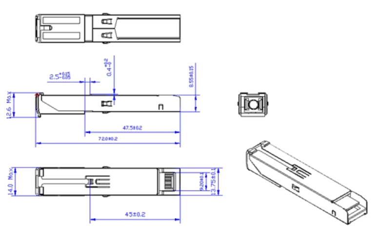
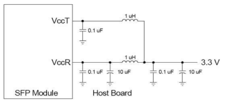
Recommended Host Board Power Supply Circuit
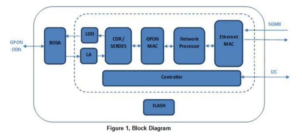
Block Diagram
| Ordering Information | |
|---|---|
| LA-GPON-ONU-34-20B-I | GPON ONU Stick with MAC SFP 1310nm-TX/1490nm-RX 1.244G-TX/2.488G-RX Class B+ 20km DOM Simplex SC/APC SMF |
| Date | Version | Description | Download |
|---|---|---|---|
| 2024-05-21 | V4.0 | Datasheet_GPON Stick_LA-GPON-ONU-34-20BD-I_V4.0.pdf | |
| Photo | Model | Description |
|---|