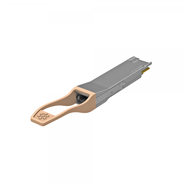
Up to 28Gbps data rate per channel, 8 duplex channels transmitters and receivers, Integrated 850nm VCSEL array and PD array, Single MPO24 connector receptacle optical interface compliant


Up to 28Gbps data rate per channel, 8 duplex channels transmitters and receivers, Integrated 850nm VCSEL array and PD array, Single MPO24 connector receptacle optical interface compliant
Features
● Up to 28Gbps data rate per channel
● 8 duplex channels transmitters and receivers
● Integrated 850nm VCSEL array and PD array
● Single MPO24 connector receptacle optical interface compliant
● Single +3.3V power supply
● DDM function implemented
● Hot-pluggable QSFP-DD form factor
● Maximum link length of 100m on 24 core MPO OM4 (MMF) fiber
● Power dissipation:<4.5W
● International class 1 laser safety certified
● Operating temperature range: 0℃ ~ +70 ℃
● Compliant with ROHS10
Absolute Maximum Ratings
|
Parameters |
Symbol |
Unit |
Min |
Max |
|
Storage Temperature Range |
Ts |
℃ |
-40 |
85 |
|
Relative Humidity |
RH |
% |
5 |
95 |
|
Power Supply Voltage |
Vcc |
V |
-0.5 |
+3.6 |
Recommended Operating Conditions
|
Parameters |
Symbol |
Unit |
Min. |
Typical |
Max |
|
Operating Case Temperature Range |
Tc |
℃ |
0 |
|
70 |
|
Power Supply Voltage |
Vcc |
V |
3.14 |
3.3 |
3.46 |
|
NRZ Bit Rate(Per channel) |
BR |
Gbps |
|
25.78 |
|
Optical Characteristics
|
Parameters |
Symbol |
Unit |
Min. |
Typical |
Max |
Note |
|
|
Transmitter(per Lane) |
|||||||
|
Signaling Speed per Lane |
|
Gbps |
25.78125 |
NRZ |
|||
|
Center wavelength |
|
nm |
840 |
850 |
860 |
|
|
|
RMS Spectral Width |
SW |
nm |
|
|
0.6 |
|
|
|
Average Launch Power per lane |
TXPx |
dBm |
-8.4 |
|
2.4 |
|
|
|
Tx OMA per lane |
TxOMA |
dBm |
-6.4 |
|
3 |
|
|
|
Difference in power between any two lane(OMA) |
DPx |
dBm |
|
|
4 |
|
|
|
Average launch power of off transmitter per lane |
|
dBm |
|
|
-30 |
|
|
|
Transmitter and Dispersion eye closure per lane |
TDEC |
dB |
|
|
4.3 |
|
|
|
Launch power in OMA minus TDEC |
|
dBm |
-7.3 |
|
|
|
|
|
Optical Extinction Ratio |
ER |
dB |
2 |
|
|
|
|
|
Optical Return Loss Tolerance |
ORL |
dB |
|
|
12 |
|
|
|
Encircled Flux |
FLX |
dBm |
>86% at 19um |
|
|||
|
<30%at 4.5um |
|
||||||
|
Relative Intensity Noise |
RIN |
dB/Hz |
|
|
RIN |
|
|
|
Receiver(per Lane) |
|||||||
|
Signaling Speed per Lane |
|
Gbps |
25.78125 |
NRZ |
|||
|
Center wavelength |
|
nm |
840 |
|
860 |
|
|
|
Damage Threshold |
DT |
dBm |
3.4 |
|
|
|
|
|
Average receive power per lane |
RXPx |
dBm |
-10.3 |
|
2.4 |
|
|
|
Receiver power (OMA) per lane |
RxOMA |
dBm |
|
|
3 |
|
|
|
Receiver reflectance |
Rfl |
dB |
|
|
-12 |
|
|
|
vertical eye closure penalty, per lane |
|
dB |
|
|
1.9 |
|
|
|
Stressed Receive Sensitivity(OMA) per lane |
SRS |
dBm |
|
|
-5.2 |
|
|
|
Sensitivity(OMA) per lane |
S |
dBm |
|
|
-10.3 |
|
|
|
LOS De-Assert |
LOSD |
dBm |
|
|
-12 |
|
|
|
LOS Assert |
LOSA |
dBm |
-30 |
|
|
|
|
|
LOS Hysteresis |
|
dBm |
0.5 |
|
|
|
|
Principle Diagram
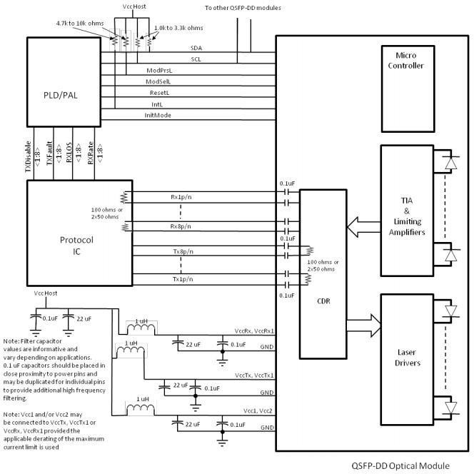
Figure 1. Module Principle Diagram
Electric Ports Definition
|
Parameters |
Symbol |
Unit |
Min. |
Typical |
Max |
Note |
|
Supply Voltage |
VCC VCC3.3-Tx VCC3.3-Rx |
V |
3.14 |
3.3 |
3.46 |
|
|
Supply Current |
Icc |
mA |
|
|
1300 |
|
|
PowerConsumptoin |
Pc |
W |
|
|
4.5 |
|
|
Transceiver Power -on Initialize Time |
|
ms |
|
|
2000 |
|
|
Transmitter |
||||||
|
Single Ended Input VoltageTolerance |
VinT |
V |
-0.3 |
|
4.0 |
|
|
Differential Data Input Swing |
VIN |
mVp-p |
300 |
|
1200 |
|
|
AC Common Mode Output Voltage(RMS) |
|
mV |
15 |
|
|
|
|
Differential Input Impedance |
|
Ω |
90 |
100 |
110 |
|
|
Receiver |
||||||
|
Single Ended Input VoltageTolerance |
VoutR |
V |
|
|
0.2 |
|
|
Differential Data Output Swing |
Vout,PP |
mVp-p |
350 |
|
850 |
|
|
AC Common Mode Output Voltage(RMS) |
|
mV |
|
|
7.5 |
|
|
Differential Output Impedance |
|
Ω |
90 |
100 |
110 |
|
|
IIC communication |
||||||
|
IIC Clock frequency |
|
KHZ |
|
100 |
400 |
|
|
clock stretching |
|
us |
|
|
500 |
|
|
Data hold time |
|
ns |
300 |
|
|
|
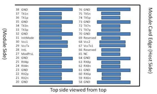
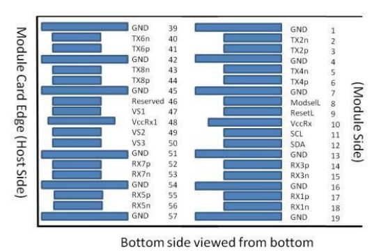
Figure 2. Electrical Pin-out Details
|
Pin |
Logic |
Symbol |
Deion |
Note |
|
1 |
|
GND |
Ground |
1 |
|
2 |
CML-I |
Tx2n |
TransmitterInvertedDataInput |
|
|
3 |
CML-I |
Tx2p |
TransmitterNon-InvertedDataInput |
|
|
4 |
|
GND |
Ground |
1 |
|
5 |
CML-I |
Tx4n |
TransmitterInvertedDataInput |
|
|
6 |
CML-I |
Tx4p |
TransmitterNon-InvertedDataInput |
|
|
7 |
|
GND |
Ground |
1 |
|
8 |
LVTTL-I |
ModSelL |
ModuleSelect |
|
|
9 |
LVTTL-I |
ResetL |
ModuleReset |
|
|
10 |
|
VccRx |
+3.3VPowerSupplyReceiver |
2 |
|
11 |
LVCOMS-I/O |
SCL |
2-WireSerialInterfaceClock |
|
|
12 |
LVCOMS-I/O |
SDA |
2-WireSerialInterfaceData |
|
|
13 |
|
GND |
Ground |
1 |
|
14 |
CML-0 |
Rx3p |
ReceiverNon-InvertedDataOutput |
|
|
15 |
CML-0 |
Rx3n |
ReceiverInvertedDataOutput |
|
|
16 |
|
GND |
Ground |
1 |
|
17 |
CML-0 |
Rx1p |
ReceiverNon-InvertedDataOutput |
|
|
18 |
CML-0 |
Rx1n |
ReceiverInvertedDataOutput |
|
|
19 |
|
GND |
Ground |
1 |
|
20 |
|
GND |
Ground |
1 |
|
21 |
CML-0 |
Rx2n |
ReceiverInvertedDataOutput |
|
|
22 |
CML-0 |
Rx2p |
ReceiverNon-InvertedDataOutput |
|
|
23 |
|
GND |
Ground |
1 |
|
24 |
CML-0 |
Rx4n |
ReceiverInvertedDataOutput |
|
|
25 |
CML-0 |
Rx4p |
ReceiverNon-InvertedDataOutput |
|
|
26 |
|
GND |
Ground |
1 |
|
27 |
LVTTL-0 |
ModPrsL |
ModulePresent |
|
|
28 |
LVTTL-0 |
IntL |
Interrupt |
|
|
29 |
|
VccTx |
+3.3VPowerSupplytransmitter |
2 |
|
30 |
|
Vcc1 |
+3.3VPowerSupply |
2 |
|
31 |
LVTTL-I |
InitMode |
Initialization mode; In legacyQSFPapplications,theIntiModepadisc alledLPMode |
|
|
32 |
|
GND |
Ground |
1 |
|
33 |
CML-I |
Tx3p |
TransmitterNon-InvertedDataInput |
|
|
34 |
CML-I |
Tx3n |
TransmitterInvertedDataInput |
|
|
35 |
|
GND |
Ground |
1 |
|
36 |
CML-I |
Tx1p |
TransmitterNon-InvertedDataInput |
|
|
37 |
CML-I |
Tx1n |
TransmitterInvertedDataInput |
|
|
38 |
|
GND |
Ground |
1 |
|
39 |
|
GND |
Ground |
1 |
|
40 |
CML-I |
Tx6n |
TransmitterInvertedDataInput |
|
|
41 |
CML-I |
Tx6p |
TransmitterNon-InvertedDataInput |
|
|
42 |
|
GND |
Ground |
1 |
|
43 |
CML-I |
Tx8n |
TransmitterInvertedDataInput |
|
|
44 |
CML-I |
Tx8p |
TransmitterNon-InvertedDataInput |
|
|
45 |
|
GND |
Ground |
1 |
|
46 |
|
Reserved |
Forfutureuse |
3 |
|
47 |
|
VS1 |
ModuleVendorSpecific1 |
3 |
|
48 |
|
VccRx1 |
+3.3VPowerSupplyReceiver |
2 |
|
49 |
|
VS2 |
ModuleVendorSpecific2 |
3 |
|
50 |
|
VS3 |
ModuleVendorSpecific3 |
3 |
|
51 |
|
GND |
Ground |
1 |
|
52 |
CML-0 |
Rx7p |
ReceiverNon-InvertedDataOutput |
|
|
53 |
CML-0 |
Rx7n |
ReceiverInvertedDataOutput |
|
|
54 |
|
GND |
Ground |
1 |
|
55 |
CML-0 |
Rx5p |
ReceiverNon-InvertedDataOutput |
|
|
56 |
CML-0 |
Rx5n |
ReceiverInvertedDataOutput |
|
|
57 |
|
GND |
Ground |
1 |
|
58 |
|
GND |
Ground |
1 |
|
59 |
CML-0 |
Rx6n |
ReceiverInvertedDataOutput |
|
|
60 |
CML-0 |
Rx6p |
ReceiverNon-InvertedDataOutput |
|
|
61 |
|
GND |
Ground |
1 |
|
62 |
CML-0 |
Rx8n |
ReceiverInvertedDataOutput |
|
|
63 |
CML-0 |
Rx8p |
ReceiverNon-InvertedDataOutput |
|
|
64 |
|
GND |
Ground |
1 |
|
65 |
|
NC |
NotConnect |
3 |
|
66 |
|
Reserved |
Forfutureuse |
3 |
|
67 |
|
VccTx1 |
+3.3VPowerSupplytransmitter |
2 |
|
68 |
|
Vcc2 |
+3.3VPowerSupply |
2 |
|
70 |
|
GND |
Ground |
1 |
|
71 |
CML-I |
Tx7p |
TransmitterNon-InvertedDataInput |
|
|
72 |
CML-I |
Tx7n |
TransmitterInvertedDataInput |
|
|
73 |
|
GND |
Ground |
1 |
|
74 |
CML-I |
Tx5p |
TransmitterNon-InvertedDataInput |
|
|
75 |
CML-I |
Tx5n |
TransmitterInvertedDataInput |
|
|
76 |
|
GND |
Ground |
1 |
Notes:
1.QSFP-DD uses common ground (GND) for all signals and supply (power). All the common within the QSFP-DD module and all module voltages are referenced to this potential unless otherwise noted. Connected theses directly to the host board signal common ground plane.
2.VccRx, VccRx1, Vcc1, Vcc2, VccTx, and VccTx1 shall be applied concurrently. Requirements defined for the host side of the Host Card Edge Connector are listed in Table 4. VccRx, VccRx1, Vcc1, Vcc2, VccTx, and VccTx1 may be internally connected within the module in any combination. The connector Vcc pins are each rated for a maximum current of 1000mA.
3.All Vendor Specific, Reserved and No Connect pins may be terminated with 50 ohms to ground on the host. Pad 65 (No Connect) shall be left unconnected within the module. Vendor Specific and Reserved pads shall have an impedance to GND that is greater than 10 kOhms and less than 100pF.
Digital Diagnostic Memory Map
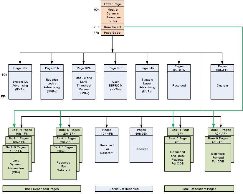
Figure 3 Digital Diagnostic Memory Map
Host Board Power Supply Filtering
Any voltage drop across a filter network on the host is counted against the host DC set point accuracy specification. Inductors with DC Resistance of less than 0.1 Ohm should be used in order to maintain the required voltage at the Host Edge Card Connector. Figure is the suggested transceiver/host interface.
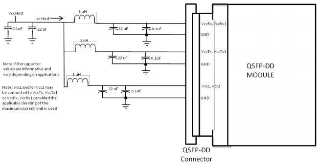
Figure 4 Recommended Host Board Power Supply Filtering
Outline Drawing (mm)
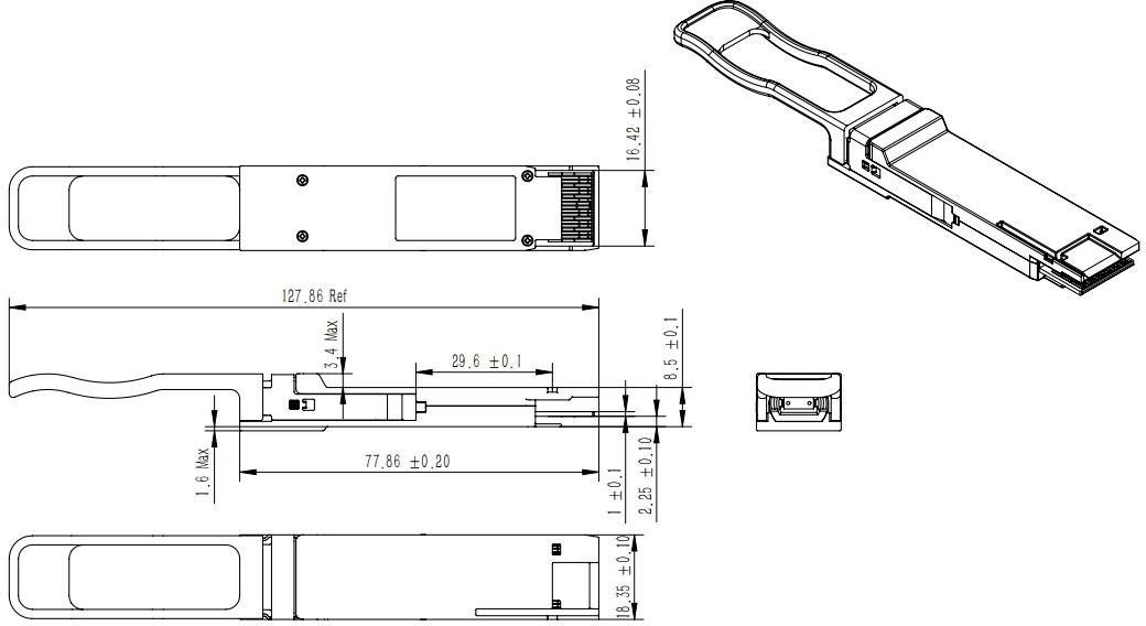
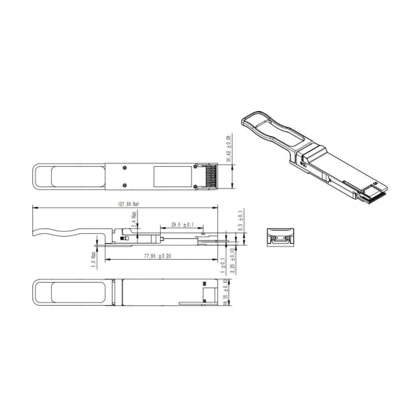
Figure 5 Package Outline
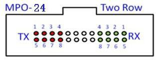
Figure 6 MPO Pinout Diagram and Deion
Host PCB layout recommendation

Figure 7 PCB Layout Recommendation
Applications
● 200GBASE-SR8 Ethernet
● 2×100GBASE-SR4 Ethernet
● Switch & Router Connections
● Data Centers
● Other 200G Interconnect Requirements
| Ordering Information |
|---|
| Date | Version | Description | Download |
|---|---|---|---|
| 2024-04-26 | V1.0 | Datasheet_200G QSFP-DD SR8 850nm 100m _LA-OT-200G-SR8_V2.X.pdf | |
| Photo | Model | Description |
|---|