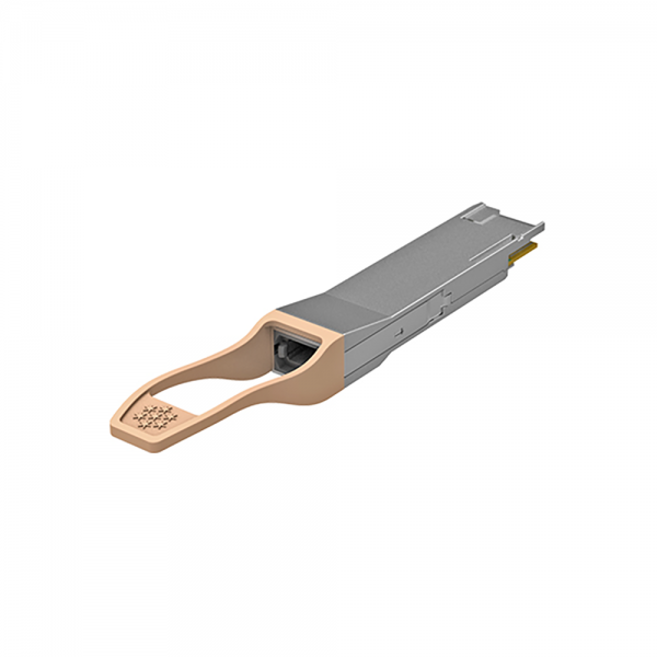
This product is a 200Gb/s transceiver module designed for 10km optical communication applications. The design is compliant to IEEE802.3bs 200GBASE-LR4 standard.
This product is a 200Gb/s transceiver module designed for 10km optical communication applications. The design is compliant to IEEE802.3bs 200GBASE-LR4 standard.
This product is a 200Gb/s transceiver module designed for 10km optical communication applications. The design is compliant to IEEE802.3bs 200GBASE-LR4 standard. For 200GAUI-8 Electrical interface, the module converts 8 input channels(ch) of 25Gb/s electrical data to 4 channels of LWDM optical signals, and multiplexes them into a single channel for 200Gb/s (PAM4) optical transmission. Reversely, on the receiver side, the module optically de-multiplexes a 200Gb/s(PAM4) input into 4 LWDM channels of signals, and converts them to 8 channels output electrical data. For 200GAUI-4 Electrical interface, the module converts 4 input channels(ch) of 50Gb/s electrical data to 4 channels of LWDM optical signals, and multiplexes them into a single channel for 200Gb/s (PAM4) optical transmission. Reversely, on the receiver side, the module optically de-multiplexes a 200Gb/s(PAM4) input into 4 LWDM channels of signals, and converts them to 4 channels output electrical data. The central wavelengths of the 4 LWDM channels. It contains a duplex LC connector for the optical interface and a 76-pin connector for the electrical interface. To minimize the optical dispersion in the long-haul system, single-mode fiber (SMF) has to be applied in this module. Host FEC is required to support up to 10km fiber transmission. The product is designed with form factor, optical/electrical connection and digital diagnostic interface according to the QSFP-DD Multi-Source Agreement (MSA). It has been designed to meet the harshest external operating conditions including temperature, humidity and EMI interference.
Features
● IEEE802.3bs compliant
● QSFP-DD MSA compliant
● 4 LWDM lanes MUX/DEMUX design
● Supports 212.5Gb/s aggregate bit rate
● Up to 10km transmission on single mode fiber (SMF) with FEC
● Operating case temperature: 0 to 70oC
● 200GAUI-8 and 200GAUI-4 electrical interface
● Maximum power consumption 10.8W
● LC duplex connector
● RoHS compliant
Transceiver Block Diagram
For 200GAUI-8

For 200GAUI-4
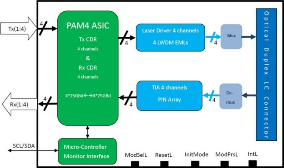
Figure 1. Transceiver Block Diagram
Pin Assignment and Deion
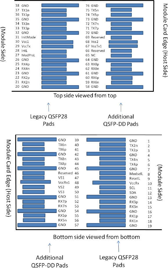
Figure 2. MSA compliant Connector
Pin Definition
|
Pin |
Logic |
Symbol |
Deion |
Plug Sequence |
Notes |
|
1 |
|
GND |
Ground |
1B |
1 |
|
2 |
CML-I |
Tx2n |
Transmitter Inverted Data Input |
3B |
|
|
3 |
CML-I |
Tx2p |
Transmitter Non-Inverted Data Input |
3B |
|
|
4 |
|
GND |
Ground |
1B |
1 |
|
5 |
CML-I |
Tx4n |
Transmitter Inverted Data Input |
3B |
|
|
6 |
CML-I |
Tx4p |
Transmitter Non-Inverted Data Input |
3B |
|
|
7 |
|
GND |
Ground |
1B |
1 |
|
8 |
LVTTL-I |
ModSelL |
Module Select |
3B |
|
|
9 |
LVTTL-I |
ResetL |
Module Reset |
3B |
|
|
10 |
|
VccRx |
+3.3V Power Supply Receiver |
2B |
2 |
|
11 |
LVCMOS-
I/O |
SCL |
2-wire serial interface clock |
3B |
|
|
12 |
LVCMOS-
I/O |
SDA |
2-wire serial interface data |
3B |
|
|
13 |
|
GND |
Ground |
1B |
1 |
|
14 |
CML-O |
Rx3p |
Receiver Non-Inverted Data Output |
3B |
|
|
15 |
CML-O |
Rx3n |
Receiver Inverted Data Output |
3B |
|
|
16 |
GND |
Ground |
1B |
|
1 |
|
17 |
CML-O |
Rx1p |
Receiver Non-Inverted Data Output |
3B |
|
|
18 |
CML-O |
Rx1n |
Receiver Inverted Data Output |
3B |
|
|
19 |
|
GND |
Ground |
1B |
1 |
|
20 |
|
GND |
Ground |
1B |
1 |
|
21 |
CML-O |
Rx2n |
Receiver Inverted Data Output |
3B |
|
|
22 |
CML-O |
Rx2p |
Receiver Non-Inverted Data Output |
3B |
|
|
23 |
|
GND |
Ground |
1B |
1 |
|
24 |
CML-O |
Rx4n |
Receiver Inverted Data Output |
3B |
|
|
25 |
CML-O |
Rx4p |
Receiver Non-Inverted Data Output |
3B |
|
|
26 |
|
GND |
Ground |
1B |
1 |
|
27 |
LVTTL-O |
ModPrsL |
Module Present |
3B |
|
|
28 |
LVTTL-O |
IntL |
Interrupt |
3B |
|
|
29 |
|
VccTx |
+3.3V Power supply transmitter |
2B |
2 |
|
30 |
|
Vcc1 |
+3.3V Power supply |
2B |
2 |
|
31 |
LVTTL-I |
InitMode |
Initialization mode; In legacy QSFP applications, the InitMode pad is
called LPMODE |
3B |
|
|
32 |
|
GND |
Ground |
1B |
1 |
|
33 |
CML-I |
Tx3p |
Transmitter Non-Inverted Data Input |
3B |
|
|
34 |
CML-I |
Tx3n |
Transmitter Inverted Data Input |
3B |
|
|
35 |
|
GND |
Ground |
1B |
1 |
|
36 |
CML-I |
Tx1p |
Transmitter Non-Inverted Data Input |
3B |
|
|
37 |
CML-I |
Tx1n |
Transmitter Inverted Data Input |
3B |
|
|
38 |
|
GND |
Ground |
1B |
1 |
|
39 |
|
GND |
Ground |
1A |
1 |
|
40 |
CML-I |
Tx6n |
Transmitter Inverted Data Input |
3A |
|
|
41 |
CML-I |
Tx6p |
Transmitter Non-Inverted Data Input |
3A |
|
|
42 |
|
GND |
Ground |
1A |
1 |
|
43 |
CML-I |
Tx8n |
Transmitter Inverted Data Input |
3A |
|
|
44 |
CML-I |
Tx8p |
Transmitter Non-Inverted Data Input |
3A |
|
|
45 |
|
GND |
Ground |
1A |
1 |
|
46 |
|
Reserved |
For future use |
3A |
3 |
|
47 |
|
VS1 |
Module Vendor Specific 1 |
3A |
3 |
|
48 |
|
VccRx1 |
3.3V Power Supply |
2A |
2 |
|
49 |
|
VS2 |
Module Vendor Specific 2 |
3A |
3 |
|
50 |
|
VS3 |
Module Vendor Specific 3 |
3A |
3 |
|
51 |
|
GND |
Ground |
1A |
1 |
|
52 |
CML-O |
Rx7p |
Receiver Non-Inverted Data Output |
3A |
|
|
53 |
CML-O |
Rx7n |
Receiver Inverted Data Output |
3A |
|
|
54 |
|
GND |
Ground |
1A |
1 |
|
55 |
CML-O |
Rx5p |
Receiver Non-Inverted Data Output |
3A |
|
|
56 |
CML-O |
Rx5n |
Receiver Inverted Data Output |
3A |
|
|
57 |
|
GND |
Ground |
1A |
1 |
|
58 |
|
GND |
Ground |
1A |
1 |
|
59 |
CML-O |
Rx6n |
Receiver Inverted Data Output |
3A |
|
|
60 |
CML-O |
Rx6p |
Receiver Non-Inverted Data Output |
3A |
|
|
61 |
|
GND |
Ground |
1A |
1 |
|
62 |
CML-O |
Rx8n |
Receiver Inverted Data Output |
3A |
|
|
63 |
CML-O |
Rx8p |
Receiver Non-Inverted Data Output |
3A |
|
|
64 |
|
GND |
Ground |
1A |
1 |
|
65 |
|
NC |
No Connect |
3A |
3 |
|
66 |
|
Reserved |
For future use |
3A |
3 |
|
67 |
|
VccTx1 |
3.3V Power Supply |
2A |
2 |
|
68 |
|
Vcc2 |
3.3V Power Supply |
2A |
2 |
|
69 |
|
Reserved |
For Future Use |
3A |
3 |
|
70 |
|
GND |
Ground |
1A |
1 |
|
71 |
CML-I |
Tx7p |
Transmitter Non-Inverted Data Input |
3A |
|
|
72 |
CML-I |
Tx7n |
Transmitter Inverted Data Input |
3A |
|
|
73 |
|
GND |
Ground |
1A |
1 |
|
74 |
CML-I |
Tx5p |
Transmitter Non-Inverted Data Input |
3A |
|
|
75 |
CML-I |
Tx5n |
Transmitter Inverted Data Input |
3A |
|
|
76 |
|
GND |
Ground |
1A |
1 |
Notes:
1. GND is the symbol for signal and supply (power) common for QSFP-DD modules. All are common within the QSFP-DD module and all module voltages are referenced to this potential unless otherwise noted. Connect these directly to the host board signal common ground plane.
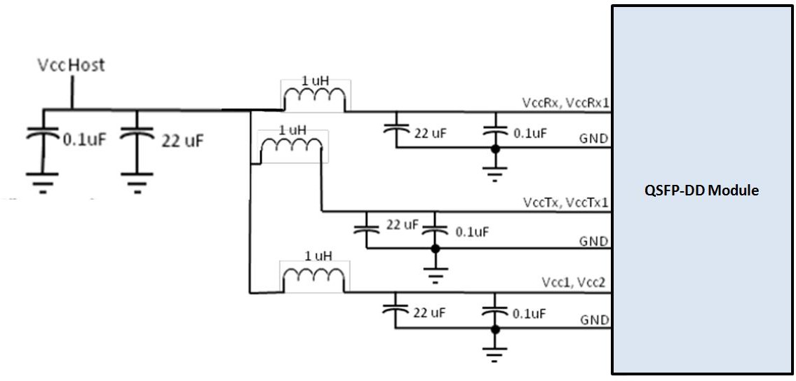
2. VccRx, Vcc1 and VccTx are the receiving and transmission power suppliers and shall be applied concurrently. Recommended host board power supply filtering is shown in Figure 3 below. Vcc Rx, Vcc1 and Vcc Tx may be internally connected within the QSFP-DD transceiver module in any combination. The connector pins are each rated for a maximum current of 1000mA.
Recommended Power Supply Filter
Absolute Maximum Ratings
It has to be noted that the operation in excess of any individual absolute maximum ratings might cause permanent damage to this module.
|
Parameter |
Symbol |
Min |
Max |
Units |
Notes |
|
Storage Temperature |
TS |
-40 |
85 |
degC |
|
|
Operating Case Temperature |
TOP |
0 |
70 |
degC |
|
|
Power Supply Voltage |
VCC |
-0.5 |
3.6 |
V |
|
|
Relative Humidity (non-condensation) |
RH |
0 |
85 |
% |
|
|
Damage Threshold, each Lane |
THd |
3.5 |
|
dBm |
|
Recommended Operating Conditions and Power Supply Requirements
|
Parameter |
Symbol |
Min |
Typical |
Max |
Units |
Notes |
|
Operating Case Temperature |
TOP |
0 |
|
70 |
degC |
|
|
Power Supply Voltage |
VCC |
3.135 |
3.3 |
3.465 |
V |
|
|
Data Rate, each Lane |
|
|
26.5625 |
|
GBd |
|
|
|
53.125 |
|
Gb/s |
|
||
|
Data Rate Accuracy |
|
-100 |
|
100 |
ppm |
|
|
Pre-FEC Bit Error Ratio |
|
|
|
2.4x10⁻⁴ |
|
|
|
Post-FEC Bit Error Ratio |
|
|
|
1x10-12 |
|
1 |
|
Control Input Voltage High |
|
2 |
|
Vcc |
V |
|
|
Control Input Voltage Low |
|
0 |
|
0.8 |
V |
|
|
Link Distance with G.652 |
D |
0.002 |
|
10 |
km |
2 |
Notes:
1. FEC provided by host system.
2. FEC required on host system to support maximum distance.
Electrical Characteristics
The following electrical acteristics are defined over the Recommended Operating Environment unless otherwise specified.
|
Parameter |
Symbol |
Min |
Typical |
Max |
Units |
Notes |
||
|
Power Consumption |
|
|
|
10.8 |
W |
|
||
|
Supply Current |
Icc |
|
|
3258 |
mA |
|
||
|
Transmitter (each Lane) |
||||||||
|
Signaling rate per lane(200GBASE-LR4) |
|
26.5625±100ppm |
GBd |
|
||||
|
Peak-to-peak differential output voltage |
|
|
|
900 |
mv |
|
||
|
AC common-mode
output voltage |
|
17.5 mV RMS with respect
to signal ground |
mV |
|
||||
|
Differential output return loss |
|
Meets Equation (120D-2) constraints |
|
|
||||
|
Reference impedance for output return loss |
|
100 |
Ω |
|
||||
|
Common to differential mode conversion |
Zin |
Meets Equation (83E–3) constraints |
|
|
||||
|
Differential termination mismatch |
|
Less than 10% |
|
|
||||
|
Transition time |
|
Greater than or equal to 12 ps |
|
|
||||
|
Eye width |
|
0.57 |
UI |
|
||||
|
Eye height |
|
228 |
mV |
|
||||
|
Crosstalk source |
|
Asynonous crosstalk source using Pattern 5, Pattern 3, or valid 200GBASE-R signal |
|
|
||||
|
Vertical eye closure |
|
|
|
5.5 |
dB |
|
||
|
Receiver (each Lane) |
||||||||
|
Single-ended Output Voltage |
|
-0.4 |
|
3.3 |
V |
Referred to signal
common |
||
|
Differential pk-pk input |
|
900 |
|
|
mV |
|
||
|
voltage tolerance |
||||||||
|
|
|
Equati |
|
|
|
|
||
|
Differential input return |
on |
|||||||
|
loss |
(83E– |
|||||||
|
|
5) |
|||||||
|
|
|
Equati |
|
|
|
|
||
|
Differential to common- |
on |
|||||||
|
mode input returnloss |
(83E– |
|||||||
|
|
6) |
|||||||
|
Termination Mismatch at |
|
|
|
10 |
% |
|
||
|
1MHz |
||||||||
|
Module stressed input |
|
|
|
|
||||
|
test |
See 83E.3.4.1 |
|||||||
|
DC common mode |
|
|
|
|
|
|
||
|
voltage |
-350 |
2850 |
mv |
|||||
|
Eye width |
|
0.46 |
UI |
|
||||
|
Eye height |
|
95 |
mV |
|
||||
200GAUI-4 Electrical Characteristics
|
Parameter |
Symbol |
Min |
Typical |
Max |
Units |
Notes |
|
|
Power Consumption |
|
|
|
10.8 |
W |
|
|
|
Supply Current |
Icc |
|
|
3258 |
mA |
|
|
|
Transmitter (each Lane) |
|||||||
|
Signaling rate per
lane(200GBASE-LR4) |
|
26.5625±100ppm |
GBd |
|
|||
|
Peak-to-peak differential
output voltage |
|
|
|
900 |
mv |
|
|
|
AC common-mode
output voltage |
|
|
|
17.5 |
mV |
|
|
|
Differential output return
loss |
|
Equation (83E-2) |
|
|
|||
|
Common to differential
mode conversion |
Zin |
Equation (83E–3) |
|
|
|||
|
Differential termination
mismatch |
|
|
|
10 |
% |
|
|
|
Transition time(20% to
80%) |
|
9.5 |
|
|
ps |
|
|
|
DC common mode
voltage |
|
-350 |
|
2850 |
mV |
|
|
|
Receiver (each Lane) |
|||||||
|
Single-ended Output Voltage |
|
-0.4 |
|
3.3 |
V |
Referred to signal
common |
|
|
Differential pk-pk input
voltage tolerance |
|
900 |
|
|
mV |
|
|
|
Differential input return loss |
|
Equati on (83E–
5) |
|
|
|
|
|
|
Differential to common- mode input returnloss |
|
Equati on
(83E– |
|
|
|
|
|
Optical Characteristics
|
Parameter |
Symbol |
Min |
Typical |
Max |
Units |
Notes |
|
Wavelength Assignment |
L0 |
1294.53 |
1295.56 |
1296.59 |
nm |
|
|
L1 |
1299.02 |
1300.05 |
1301.09 |
nm |
|
|
|
L2 |
1303.54 |
1304.58 |
1305.63 |
nm |
|
|
|
L3 |
1308.09 |
1309.14 |
1310.19 |
nm |
|
|
|
Transmitter |
||||||
|
Data Rate, each Lane |
|
26.5625 ± 100 ppm |
GBd |
|
||
|
Modulation Format |
|
PAM4 |
|
|
||
|
Side-mode Suppression Ratio |
SMSR |
30 |
|
|
dB |
Modulated |
|
Total Average Launch Power |
PT |
|
|
11.3 |
dBm |
|
|
Average Launch Power, each
Lane |
PAVG |
-3.4 |
|
5.3 |
dBm |
1 |
|
Outer Optical Modulation
Amplitude (OMAouter), each Lane |
POMA |
-0.4 |
|
5.1 |
dBm |
2 |
|
Launch Power in OMAouter minus TDECQ, each Lane |
|
-1.8 |
|
|
dB |
For ER
≥4.5dB |
|
-1.7 |
|
|
dB |
For ER <4.5dB |
||
|
Transmitter and Dispersion Eye Clouser for PAM4, each Lane |
TDECQ |
|
|
3.4 |
dB |
|
|
Extinction Ratio |
ER |
3.5 |
|
|
dB |
|
|
Difference in Launch Power between any Two Lanes
(OMAouter) |
|
|
|
4 |
dB |
|
|
RIN16.5OMA |
RIN |
|
|
-132 |
dB/Hz |
|
|
Optical Return Loss Tolerance |
TOL |
|
|
15.1 |
dB |
|
|
Transmitter Reflectance |
TR |
|
|
-26 |
dB |
|
|
Average Launch Power of OFF
Transmitter, each Lane |
Poff |
|
|
-30 |
dBm |
|
|
Receiver |
||||||
|
|
26.5625 ± 100 ppm |
GBd |
|
|
|
|
|
|
PAM4 |
|
|
|
|
|
|
THd |
6.3 |
|
|
dBm |
3 |
|
|
|
-9.7 |
|
5.3 |
dBm |
4 |
|
|
|
|
|
5.1 |
dBm |
|
|
|
Difference in Receiver Power between any Two Lanes |
|
|
|
4.2 |
dB |
|
|
SEN |
|
|
For BER
of 2.4E-4 |
|||
|
Stressed Receiver Sensitivity |
SRS |
|
|
|
||
|
RR |
|
|
||||
|
LOSA |
-25.7 |
|
||||
|
LOSD |
|
|
||||
|
LOSH |
|
|||||
|
|
|
|||||
|
|
-1 |
|||||
|
Notes:
1. Average launch power, each lane (min) is informative and not the principal indicator of signal strength. A transmitter with launch power below this value cannot be compliant; however, a value above this does not ensure compliance.
2. Even if the TDECQ < 1.4 dB for an extinction ratio of ≥ 4.5 dB or TDECQ < 1.3 dB for an extinction ratio of < 4.5 dB, the OMAouter (min) must exceed the minimum value specified here.
The receiver shall be able to tolerate, without damage, continuous exposure to an optical input signal having this average power level.
3. Average receive power, each lane (min) is informative and not the principal indicator of signal strength. A received power below this value cannot be compliant; however, a value above this does not ensure compliance.
4. Measured with conformance test signal for BER = 2.4x10⁻⁴.
5. These test conditions are for measuring stressed receiver sensitivity. They are not acteristics of the receiver. |
||||||
Digital Diagnostic Functions
The following digital diagnostic acteristics are defined over the normal operating conditions unless otherwise specified.
|
Parameter |
Symbol |
Min |
Max |
Units |
Notes |
|
Temperature monitors absolute error |
DMI_Temp |
-3 |
3 |
degC |
Over operating temperature range |
|
Supply voltage monitor
absolute error |
DMI _VCC |
-0.1 |
0.1 |
V |
Over full operating range |
|
Channel RX power monitor absolute error |
DMI_RX_Ch |
-3 |
3 |
dB |
|
|
Channel Bias current monitor |
DMI_Ibias_Ch |
-10% |
10% |
mA |
|
|
Channel TX power
monitor absolute error |
DMI_TX_Ch |
-3 |
3 |
dB |
|
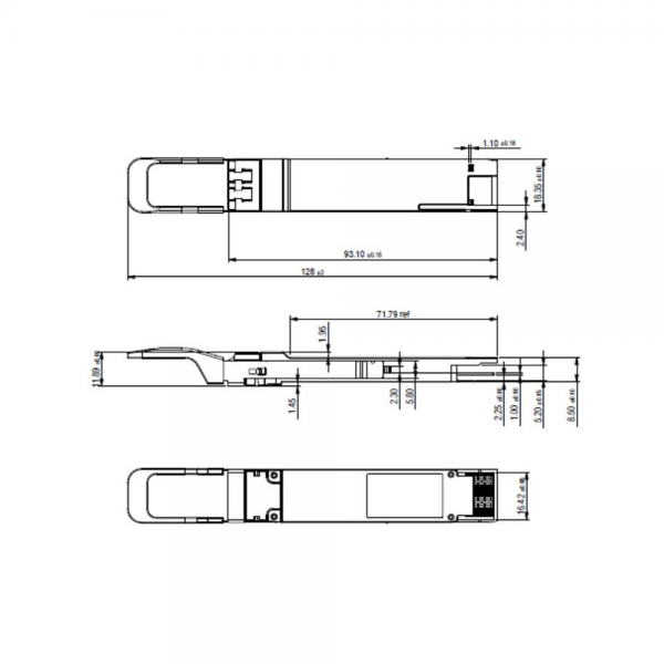
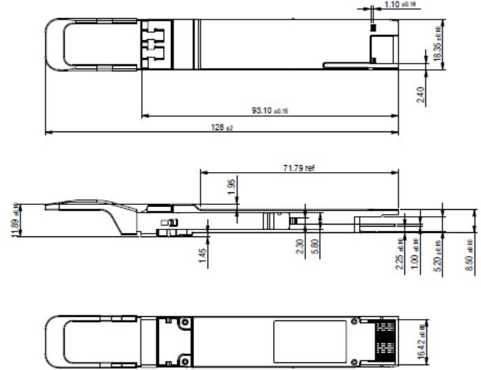
Outline Drawing (mm)
Applications
● Data Center Interconnect
● 200G Ethernet
● Enterprise networking
| Ordering Information |
|---|
| Date | Version | Description | Download |
|---|---|---|---|
| 2024-04-25 | V1.0 | Datasheet_200G QSFP-DD LR4 1310nm 10km_LA-OT-200G-LR4.pdf | |
| Photo | Model | Description |
|---|
follow us