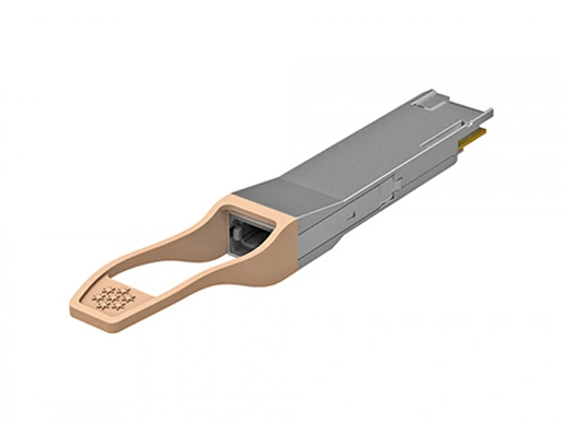
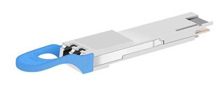
This product is a 200Gb/s Quad Small Form Factor Pluggable-double density (QSFP-DD) optical module designed for optical communication applications. The module converts 8 channels of 25Gb/s (NRZ) electrical input data to 4 channels of LAN-WDM optical signals, and multiplexes them into a single channel for 200Gb/s(PMA4) optical transmission. Reversely, on the receiver side, the module optically de-multiplexes a 200Gb/s(PMA4) optical input into 4 channels of WDM optical signals, and converts them to 8 channels of 25Gb/s (NRZ) electrical output data. The central wavelengths of the 4 LAN WDM channels are 1295.56, 1300.05, 1304.58 and 1309.14 nm as members of the LAN WDM wavelength grid defined in IEEE802.3ba. It contains a duplex LC connector for the optical interface and a 76-pin connector for the electrical interface. To minimize the optical dispersion in the long-haul system, single-mode fiber (SMF) has to be applied in this module. It can support up to 30km with 200G FEC and 40km with built-in PFEC. The product is designed with form factor, optical/electrical connection and digital diagnostic interface according to the QSFP-DD Multi-Source Agreement (MSA). It has been designed to meet the harshest external operating conditions including temperature, humidity and EMI interference.
Features
● QSFP-DD MSA compliant
● 4 LWDM lanes MUX/DEMUX design
● Up to 40km transmission on single mode fiber (SMF) with built-in PFEC
● Operating case temperature: 0 to 70oC
● Maximum power consumption 12W
● Duplex LC connector
● RoHS compliant
Transceiver Block Diagram
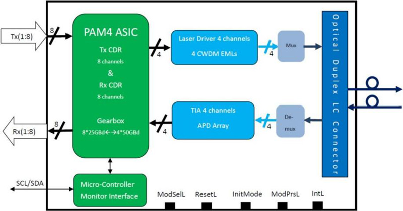
Figure 1. Transceiver Block Diagram
Pin Assignment and Deion
The electrical pinout of the QSFP-DD module is shown in Figure 2 below.
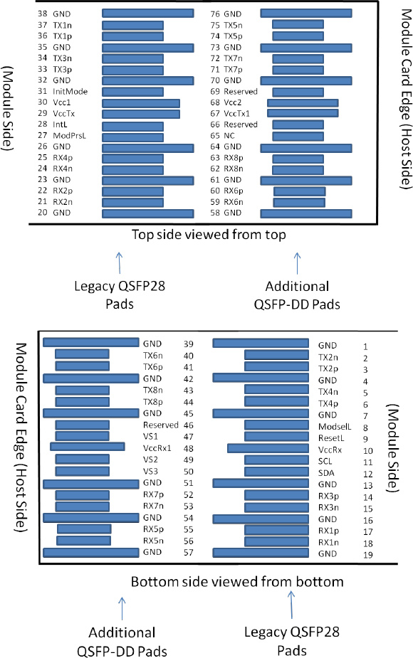
Figure 2. MSA Compliant Connector
Pin Definition
37 | CML-I | Tx1n | Transmitter Inverted Data Input | 3B |
|
38 |
| GND | Ground | 1B | 1 |
39 |
| GND | Ground | 1A | 1 |
40 | CML-I | Tx6n | Transmitter Inverted Data Input | 3A |
|
41 | CML-I | Tx6p | Transmitter Non-Inverted Data Input | 3A |
|
42 |
| GND | Ground | 1A | 1 |
43 | CML-I | Tx8n | Transmitter Inverted Data Input | 3A |
|
44 | CML-I | Tx8p | Transmitter Non-Inverted Data Input | 3A |
|
45 |
| GND | Ground | 1A | 1 |
46 |
| Reserved | For future use | 3A | 3 |
47 |
| VS1 | Module Vendor Specific 1 | 3A | 3 |
48 |
| VccRx1 | 3.3V Power Supply | 2A | 2 |
49 |
| VS2 | Module Vendor Specific 2 | 3A | 3 |
50 |
| VS3 | Module Vendor Specific 3 | 3A | 3 |
51 |
| GND | Ground | 1A | 1 |
52 | CML-O | Rx7p | Receiver Non-Inverted Data Output | 3A |
|
53 | CML-O | Rx7n | Receiver Inverted Data Output | 3A |
|
54 |
| GND | Ground | 1A | 1 |
55 | CML-O | Rx5p | Receiver Non-Inverted Data Output | 3A |
|
56 | CML-O | Rx5n | Receiver Inverted Data Output | 3A |
|
57 |
| GND | Ground | 1A | 1 |
58 |
| GND | Ground | 1A | 1 |
59 | CML-O | Rx6n | Receiver Inverted Data Output | 3A |
|
60 | CML-O | Rx6p | Receiver Non-Inverted Data Output | 3A |
|
61 |
| GND | Ground | 1A | 1 |
62 | CML-O | Rx8n | Receiver Inverted Data Output | 3A |
|
63 | CML-O | Rx8p | Receiver Non-Inverted Data Output | 3A |
|
64 |
| GND | Ground | 1A | 1 |
65 |
| NC | No Connect | 3A | 3 |
66 |
| Reserved | For future use | 3A | 3 |
67 |
| VccTx1 | 3.3V Power Supply | 2A | 2 |
68 |
| Vcc2 | 3.3V Power Supply | 2A | 2 |
69 |
| Reserved | For Future Use | 3A | 3 |
70 |
| GND | Ground | 1A | 1 |
71 | CML-I | Tx7p | Transmitter Non-Inverted Data Input | 3A |
|
72 | CML-I | Tx7n | Transmitter Inverted Data Input | 3A |
|
73 |
| GND | Ground | 1A | 1 |
74 | CML-I | Tx5p | Transmitter Non-Inverted Data Input | 3A |
|
75 | CML-I | Tx5n | Transmitter Inverted Data Input | 3A |
|
76 |
| GND | Ground | 1A | 1 |
Recommended Power Supply Filter
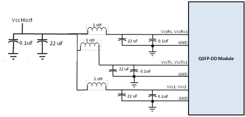
Figure 3. Recommended Power Supply Filter
Absolute Maximum Ratings
It has to be noted that the operation in excess of any individual absolute maximum ratings might cause permanent damage to this module.
Parameter | Symbol | Min | Max | Units | Notes |
Storage Temperature | TS | -40 | 85 | degC |
|
Operating Case Temperature | TOP | 0 | 70 | degC |
|
Power Supply Voltage | VCC | -0.5 | 3.6 | V |
|
Relative Humidity (non-condensation) | RH | 0 | 85 | % |
|
Damage Threshold, each Lane | THd | -5.0 |
| dBm |
|
Recommended Operating Conditions and Power Supply Requirements
Parameter | Symbol | Min | Typical | Max | Units | Notes |
Operating Case Temperature | TOP | 0 |
| 70 | degC |
|
Power Supply Voltage | VCC | 3.135 | 3.3 | 3.465 | V |
|
Data Rate, each Lane |
|
| 26.5625 |
| GBd | PAM4 |
Data Rate Accuracy |
| -100 |
| 100 | ppm |
|
Pre-FEC Bit Error Ratio |
|
|
| 2.4x10⁻⁴ |
|
|
Post-FEC Bit Error Ratio |
|
|
| 1x10-12 |
| 1 |
Link Distance | D | 0.002 |
| 30 | km | 2 |
Link Distance | D | 0.002 |
| 40 | Km | 3 |
Notes:
1. FEC provided by host system.
2. FEC required on host system to support maximum distance.
3. Built-in PFEC is required to support up to 40km
Electrical Characteristics
The following electrical acteristics are defined over the Recommended Operating Environment unless otherwise specified.
Parameter | Test Point | Min | Typical | Max | Units | Notes |
|
|
|
|
12 | SupplyCurrent | 3.64 | SignalingRate,eachLane | 26.5625± 100ppm | Differential InputVoltageTolerance | 900 |
|
| 1 |
|
Termination Mismatch | 10 | DifferentialInputReturnLoss |
IEEE802.3- Equation dB |
|
|
|
|
|
|
|
TP1 | 2015 (83E-6) |
|
|
<span font-size:14px;"="" style="box-sizing: border-box">dB |
|
|
|
|
|
|
Module Stressed Input Test | TP1a | See IEEE 802.3bs 120E.3.4.1 |
| 2 |
|
|
|
|
Single-ended Voltage Tolerance Range (Min) | TP1a | -0.4 to 3.3 | V |
|
|
|
|
|
DC Common Mode Input Voltage | TP1 | -350 |
| 2850 |
|
|
|
|
Receiver (each Lane) |
|
|
|
|
Signaling Rate, each lane | TP4 | 26.5625 ± 100 ppm | GBd |
|
|
|
|
|
Differential Peak-to-Peak Output Voltage | TP4 |
|
| 900 |
|
|
|
|
Differential Termination Mismatch | TP4 |
|
| 10 |
|
|
|
|
Differential Output Return Loss |
TP4 | IEEE 802.3- 2015 Equation (83E-2) |
|
|
|
|
|
|
Common to Differential Mode Conversion Return Loss |
TP4 | IEEE 802.3- 2015 Equation (83E-3) |
|
|
|
|
|
|
Transition Time, 20% to 80% | TP4 | 9.5 |
|
|
|
|
|
|
Near-end Eye Symmetry Mask Width (ESMW) | TP4 |
| 0.265 |
|
|
|
|
|
Near-end Eye Height, Differential | TP4 | 70 |
|
|
|
|
|
|
Far-end Eye Symmetry Mask Width (ESMW) | TP4 |
| 0.2 |
|
|
|
|
|
Far-end Eye Height, Differential | TP4 | 30 |
|
|
|
|
|
|
Far-end Pre-cursor ISI Ratio | TP4 | -4.5 |
| 2.5 |
|
|
|
|
Common Mode Output Voltage (Vcm) | TP4 | -350 |
| 2850 |
|
|
|
|
Notes:
1. With the exception to IEEE 802.3bs 120E.3.1.2 that the pattern is PRBS31Q or scrambled idle.
2. Meets BER specified in IEEE 802.3bs 120E.1.1.
3. DC common mode voltage generated by the host. Specification includes effects of ground offset voltage.
Optical Characteristics
Parameter | Symbol | Min | Typical | Max | Units | Notes |
Wavelength Assignment | L0 | 1294.53 | 1295.56 | 1296.59 | nm |
|
L1 | 1299.02 | 1300.05 | 1301.09 | nm |
|
L2 | 1303.54 | 1304.58 | 1305.63 | nm |
|
L3 | 1308.09 | 1309.14 | 1310.19 | nm |
|
Transmitter |
Data Rate, each Lane |
| 53.125 ± 100 ppm | GBd |
|
Modulation Format |
| PAM4 |
|
|
Side-mode Suppression Ratio | SMSR | 30 |
|
| dB |
|
Total Average Launch Power | PT |
|
| 14.7 | dBm |
|
Average Launch Power, each Lane | PAVG | -0.1 |
| 5.6 | dBm |
|
Outer Optical Modulation Amplitude (OMAouter), each Lane | POMA | 3.4 |
| 6.4 | dBm |
|
Launch Power in OMAouter minus TDECQ, each Lane |
| 3 |
|
| dB |
|
Transmitter and Dispersion Eye Closure for PAM4, each Lane | TDECQ |
|
| 3.2 | dB |
|
Extinction Ratio | ER | 6 |
|
| dB |
|
Difference in Launch Power between any Two Lanes (OMAouter) |
|
|
|
4 |
dB |
|
RIN15.1OMA | RIN | -132 |
|
| dB/Hz |
|
Optical Return Loss Tolerance | TOL |
|
| 15.1 | dB |
|
Transmitter Reflectance | RT |
|
| -26 | dB |
|
Average Launch Power of OFF Transmitter, each Lane | Poff |
|
| -30 | dBm |
|
Receiver |
Data Rate, each Lane |
| 53.125 ± 100 ppm | GBd |
|
Modulation Format |
| PAM4 |
|
|
Sensitivity, each lane | Sen1 | MAX (-11.1, SECQ-12.5) | dBm | For 30km |
Sensitivity, each lane | Sen2 | MAX (-14.1, SECQ-15.5) | dBm | For 40km |
Stressed Conditions for Stress Receiver Sensitivity (Note 8) |
Stressed Eye Closure for PAM4 (SECQ), Lane under Test |
|
| 3.4 |
| dB |
|
SECQ – 10*log10(Ceq), Lane under Test |
|
|
|
| dB |
|
OMAouter of each Aggressor Lane |
|
| -8 |
| dBm |
|
Digital Diagnostic Functions
Parameter | Symbol | Min | Max | Units | Notes |
Temperature Monitor Absolute Error |
DMI_Temp |
-3 |
3 |
degC | Over operating temperature range |
Supply Voltage Monitor Absolute Error | DMI _VCC | -0.1 | 0.1 | V | Over full operating range |
Channel RX Power Monitor Absolute Error |
DMI_RX_Ch |
-2 |
2 |
dB |
1 |
Channel Bias Current Monitor | DMI_Ibias_Ch | -10% | 10% | mA |
|
Channel TX Power Monitor Absolute Error | DMI_TX_Ch | -2 | 2 | dB | 1 |
The following digital diagnostic acteristics are defined over the normal operating conditions unless otherwise specified.
Notes:
4. Due to measurement accuracy of different single mode fibers, there could be an additional +/-1 dB fluctuation, or a +/- 3 dB total accuracy.
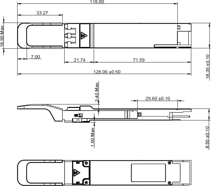
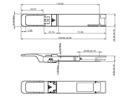
Outline Drawing (mm)
 Internet Data Center
 FAQs
FAQs Industry News
 About Us
 Data Center Switch
  Enterprise Switch
  Industrial Switch
  Access Switch
  Integrated Network
  Optical Module & Cable




 Call us on:
  Email Us:
  2106B, #3D, Cloud Park Phase 1, Bantian, Longgang, Shenzhen, 518129, P.R.C.