400G ZR QSFP-DD DCO modules are based on DP- 16QAM supporting extended C-band, polarization diversity coherent detection and advanced electronic link equalization. Chromatic dispersion compensation can be applied to the receive side of the demodulator. This module is managed utilizing the Two Wire Interface that is specified in the Common Management Interface Specification (CMIS).
The module uses a 76-pin QSFP-DD MSA QSFP-DD Hardware Specification connector for all electrical interfaces with the host card, whereas the optical interfaces on the line side are provided through the optical receptacles on the QSFP-DD. The module can be portioned into three functional parts: TX path, RX path and Control & Power block.
The host interface is comprised of a total of 8 high-speed SerDes lanes. This allows module to support one interfaces for 400G application: an independent double 4-Lane mode client interfaces (for 400GbE application) and four independent double lane mode client interfaces (for 4*100GbE application).
The management communication interface provides a number of elementary management operations that allow the host to read from or write to byte-sized management registers in the management memory map of the module. There are read and write operations both for single bytes and for contiguous byte sequences. Two types of read operations, either with implicit addressing (read from current address) or with explicit addressing, are supported.
The management communication interface distinguishes a role and a s role. The host shall be the and the module shall be the s.
The initiates all operations that lead to data transfer. Data can be transferred from the to the s (in write operations) and from the s to the (in read operations).
Features
● Support Flex-grid channel spacing DWDM in C-band
● Support Client-side Interfaces: 400GAUI-8/4*100GAUI-2
● Support Line-side DP-16QAM with CFEC
● Standard QSFP-DD type 2 form factor
● 76pin QSFP-DD MSA compliant connector
● Compliant to CMIS 5.0
● Compliant to OIF Implementation Agreement for Coherent CMIS, Rev 01.1
● OIF-400ZR-01.0_reduced2.pdf
● RoHS compliant
Typical Application
The application field of the module is widely used from short haul (ZR) to Metro(MR) interconnects. As shown in figure1, it is comprised of high-data lanes, a single 3.3V power supply, an IIC interface for module control and status report, and dedicated alarm and control pins (not shown on the figure1).
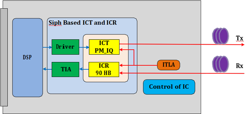
Figure 1. Transceiver Block Diagram
Host Interface
The module support for wide applications with Host interfaces: 400GAUI-8/100GUI-2. The Host interface conform to existing protocol standards and operate over standard physical layer specifications. The termination, mapping and/or aggregation of this signal is into an internal ZR frame structure. The ZR frame structure is then adapted to the CFEC engine and DSP framed for transmission over the coherent media Interface. The Host interface signaling conform to existing protocol and electrical standards as defined by IEEE 802.3TM-2018.
The Host Interface compliant to very short reach high speed chip-to-module electrical interface CEI-56G- VSR-PAM4 for PAM4 coding.
Host Interface | Application Data Rate | Lane Count | Lane Signaling Rate | Modulation |
400GAUI-8 | 425.00 Gb/s | 8 | 26.5625 GBaud (+/- 100 ppm) | PAM4 |
4*100GAUI-8 | 4*106.25 Gb/s | 8 | 26.5625 GBaud (+/- 100 ppm) | PAM4 |
Media Interface
The media interface utilizes DP-16QAM modulation, polarization diversity coherent detection, and advanced electronic link equalization with omatic dispersion and differential group delay compensation.
The module terminates the host interface signal then maps and aggregates them into an internal ZR frame structure. The ZR frame structure is then adapted to the CFEC engine and DSP framed for transmission over the coherent media interface.
Application Bit Rate | Baud Rate | Modulation | FEC |
478.75 Gb/s | 59.84375GBd | DP-16QAM | OFEC |
Host Electrical Connector & Pin Assignments
The electrical interfaces, including pad assignments for data, control, status and power supplies and host PCB layout requirements, of the module is fully compliant with the QSFP-DD MSA QSFP-DD-Hardware Specification, Rev 5.0.
The case of the QSFP-DD module is isolated from the module’s circuit ground, GND, to provide the equipment designer flexibility regarding connections between external electromagnetic interference shields and circuit ground, GND, of the module.
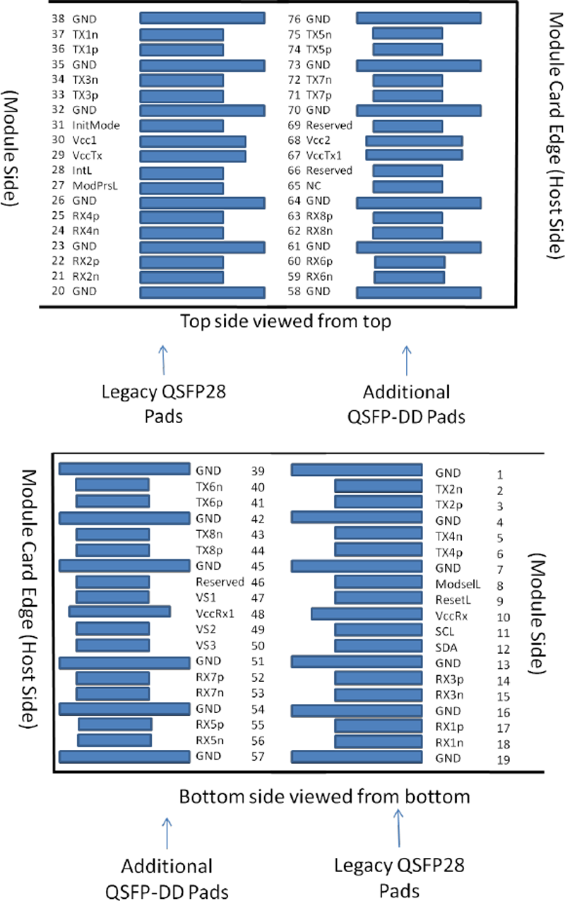
Figure 2. MSA Compliant Connector
Pin # | Logic | Symbol | Deion | Plug Sequence |
1 |
| GND | Ground | 1B |
2 | CML-I | Tx2n | Transmitter Inverted Data Input | 3B |
3 | CML-I | Tx2p | Transmitter Non-Inverted Data Input | 3B |
4 |
| GND | Ground | 1B |
5 | CML-I | Tx4n | Transmitter Inverted Data Input | 3B |
6 | CML-I | Tx4p | Transmitter Non-Inverted Data Input | 3B |
7 |
| GND | Ground | 1B |
8 | LVTTL-I | ModSelL | Module Select | 3B |
9 | LVTTL-I | ResetL | Module Reset | 3B |
10 |
| VccRx | +3.3V Power Supply Receiver | 2B |
11 | LVCMOS-I/O | SCL | 2-wire serial interface clock | 3B |
12 | LVCMOS-I/O | SDA | 2-wire serial interface data | 3B |
13 |
| GND | Ground | 1B |
14 | CML-O | Rx3p | Receiver Non-Inverted Data Output | 3B |
15 | CML-O | Rx3n | Receiver Inverted Data Output | 3B |
16 | GND | Ground | 1B |
|
17 | CML-O | Rx1p | Receiver Non-Inverted Data Output | 3B |
18 | CML-O | Rx1n | Receiver Inverted Data Output | 3B |
19 |
| GND | Ground | 1B |
20 |
| GND | Ground | 1B |
21 | CML-O | Rx2n | Receiver Inverted Data Output | 3B |
22 | CML-O | Rx2p | Receiver Non-Inverted Data Output | 3B |
23 |
| GND | Ground | 1B |
24 | CML-O | Rx4n | Receiver Inverted Data Output | 3B |
25 | CML-O | Rx4p | Receiver Non-Inverted Data Output | 3B |
26 |
| GND | Ground | 1B |
27 | LVTTL-O | ModPrsL | Module Present | 3B |
28 | LVTTL-O | IntL | Interrupt | 3B |
29 |
| VccTx | +3.3V Power supply transmitter | 2B |
30 |
| Vcc1 | +3.3V Power supply | 2B |
31 | LVTTL-I | InitMode | Initialization mode; In legacy QSFP applications, the InitMode pad is called LPMODE | 3B |
32 |
| GND | Ground | 1B |
33 | CML-I | Tx3p | Transmitter Non-Inverted Data Input | 3B |
34 | CML-I | Tx3n | Transmitter Inverted Data Input | 3B |
35 |
| GND | Ground | 1B |
36 | CML-I | Tx1p | Transmitter Non-Inverted Data Input | 3B |
37 | CML-I | Tx1n | Transmitter Inverted Data Input | 3B |
38 |
| GND | Ground | 1B |
39 |
| GND | Ground | 1A |
40 | CML-I | Tx6n | Transmitter Inverted Data Input | 3A |
41 | CML-I | Tx6p | Transmitter Non-Inverted Data Input | 3A |
42 |
| GND | Ground | 1A |
43 | CML-I | Tx8n | Transmitter Inverted Data Input | 3A |
44 | CML-I | Tx8p | Transmitter Non-Inverted Data Input | 3A |
45 |
| GND | Ground | 1A |
46 |
| Reserved | For future use | 3A |
47 |
| VS1 | Module Vendor Specific 1 | 3A |
48 |
| VccRx1 | 3.3V Power Supply | 2A |
49 |
| VS2 | Module Vendor Specific 2 | 3A |
50 |
| VS3 | Module Vendor Specific 3 | 3A |
51 |
| GND | Ground | 1A |
52 | CML-O | Rx7p | Receiver Non-Inverted Data Output | 3A |
53 | CML-O | Rx7n | Receiver Inverted Data Output | 3A |
54 |
| GND | Ground | 1A |
55 | CML-O | Rx5p | Receiver Non-Inverted Data Output | 3A |
56 | CML-O | Rx5n | Receiver Inverted Data Output | 3A |
57 |
| GND | Ground | 1A |
58 |
| GND | Ground | 1A |
59 | CML-O | Rx6n | Receiver Inverted Data Output | 3A |
60 | CML-O | Rx6p | Receiver Non-Inverted Data Output | 3A |
61 |
| GND | Ground | 1A |
62 | CML-O | Rx8n | Receiver Inverted Data Output | 3A |
63 | CML-O | Rx8p | Receiver Non-Inverted Data Output | 3A |
64 |
| GND | Ground | 1A |
65 |
| NC | No Connect | 3A |
66 |
| Reserved | For future use | 3A |
67 |
| VccTx1 | 3.3V Power Supply | 2A |
68 |
| Vcc2 | 3.3V Power Supply | 2A |
69 |
| Reserved | For Future Use | 3A |
70 |
| GND | Ground | 1A |
71 | CML-I | Tx7p | Transmitter Non-Inverted Data Input | 3A |
72 | CML-I | Tx7n | Transmitter Inverted Data Input | 3A |
73 |
| GND | Ground | 1A |
74 | CML-I | Tx5p | Transmitter Non-Inverted Data Input | 3A |
75 | CML-I | Tx5n | Transmitter Inverted Data Input | 3A |
76 |
| GND | Ground | 1A |
Absolute Maximum Ratings
It has to be noted that the operation in excess of any individual absolute maximum ratings might cause permanent damage to this module.
Parameter | Min | Max | Units | Notes |
Storage Temperature | -40 | 85 | ℃ |
|
Storage Humidity (Relative) | - | 85 | % | no-Condensing |
Case Temperature | 0 | 75 | ℃ |
|
Operating Humidity (Relative) | - | 85 | % | no-Condensing |
Short term Operating Case Temperature |
| 80 | ℃ | <24 hours |
Power Supply Absolute Range | -0.3 | 3.63 | V |
|
RX Optical Maximum Input Power | - | 10 | dBm |
|
Operating Conditions
Parameter | Min | Max | Units | Notes |
Operating Case Temperature | 0 | 75 | ℃ |
|
Operating Humidity (Relative) | - | 85 | % | no-Condensing |
Power Supply Operating Range | 3.135 | 3.465 | V |
|
RX Optical Input Power | - | 0 | dBm |
|
Power Supply
The 400G ZR QSFP-DD DCO is a Power Class 8 module. In order to avoid exceeding the host system power capacity, upon hot-plug, power cycle or reset, all QSFP-DD modules shall power up in Low Power Mode if LPMode is asserted. If LPMode is not asserted the module will proceed to High Power Mode without host intervention. Specification values for maximum instantaneous, sustained and steady state currents at each power class are given in table 5. The power supply requirements are specified in the table below.
Parameter | Min | Typical | Max | Units | Notes |
3.3V DC Power Supply Voltage | 3.135 | 3.3 | 3.465 | V |
|
3.3V DC Power Supply Current |
|
| 7 | A |
|
Power Dissipation |
|
| 18 | W |
|
Low Power Consumption |
|
| 1.5 | W |
|
Module Inrush Current |
|
| 100 | mA/us |
|
Turn-off Current
| - 100 |
|
| mA/us |
|
Power Supply Noise |
|
| 25 | mV |
|
Hardware Control and Status Pins
In addition to the 2-wire serial interface the module has the following low speed signals for control and status:
● ModSelL
● ResetL
● LPMode
● ModPrsL
● IntL
● Epps
ModSelL
The ModSelL is an input signal that shall be pulled to Vcc in the QSFP-DD module. When held low by the host, the module responds to 2-wire serial communication commands. The ModSelL allows the use of multiple QSFP-DD modules on a single 2-wire interface bus. When ModSelL is “High”, the module shall not respond to or acknowledge any 2-wire interface communication from the host.
In order to avoid conflicts, the host system shall not attempt 2-wire interface communications within the ModSelL de-assert time after any QSFP-DD modules are deed. Similarly, the host must wait at least for the period of the ModSelL assert time before communicating with the newly ed module. The assertion and de- asserting periods of different modules may overlap as long as the above timing requirements are met.
ResetL
The ResetL signal shall be pulled to Vcc in the module. A low level on the ResetL signal for longer than the minimum pulse length (t_Reset_init) initiates a complete module reset, returning all user module settings to their default state.
LPMode
LPMode is an input signal. The LPMode signal shall be pulled up to Vcc in the QSFP-DD module. LPMode is used in the control of the module power mode.
See CMIS Section 6.3.1.3.
ModPrsL
ModPrsL shall be pulled up to Vcc Host on the host board and pulled low in the module. The ModPrsL is asserted “Low” when the module is ed. The ModPrsL is deasserted “High” when the module is physically absent from the host connector due to the pull-up resistor on the host board.
Low speed signaling other than the SCL and SDA interface is based on Low Voltage TTL (LVTTL) operating at Vcc. Vcc refers to the generic supply voltages of VccTx, VccRx, Vcc host or Vcc1. Hosts shall use a pull-up resistor connected to Vcc host on each of the 2-wire interface SCL (clock), SDA (data), and all low speed status outputs. The SCL and SDA is a hot plug interface that may support a bus topology. During module ion or removal, the module may implement a pre-ge circuit which prevents corrupting data transfers from other modules that are already using the bus.
The QSFP-DD low speed electrical specifications are given in table 6. This specification ensures compatibility between host bus s and the 2-wire interface.
Parameter | Symbol | Min | Max | Unit | Condition |
SCL and SDA | VOL | 0 | 0.4 | V | IOL(max)=3 mA for fast mode, 20 mA for Fast-mode plus |
SCL and SDA | VIL | -0.3 | Vcc * 0.3 | V |
|
VIH | Vcc * 0.7 | Vcc + 0.5 | V |
|
Capacitance for SCL and SDA I/O signal | Ci |
| 14 | pF |
|
Total bus capacitive load for SCL and SDA | Cb |
| 100 | pF | For 400 kHz clock rate use 3.0k Ohms Pull-up resistor, max. |
|
| 200 | pF | For 400 kHz clock rate use 1.6k Ohms Pull-up resistor, max. |
LPMode, ResetL, ModSelL and ePPS | VIL | -0.3 | 0.8 | V |
|
VIH | 2 | Vcc + 0.3 | V |
|
LPMode, ResetL and ModSelL | |Iin| |
| 360 | uA | 0V<vin<vcc< span="" style="box-sizing: border-box"><vcc< style="box-sizing: border-box"> |
ePPS | |Iin| |
| TBD | uA | 0V<vin<vcc< span="" style="box-sizing: border-box"><vcc< style="box-sizing: border-box"> |
IntL | VOL | 0 | 0.4 | V | IOL=2.0 mA |
VOH | Vcc – 0.5 | Vcc + 0.3 | V | 10k Ohms pull-up to Host Vcc |
ModPrsL | VOL | 0 | 0.4 | V | IOL=2.0 mA |
VOH |
|
| V | ModPrsL can be implemented as a short-circuit to GND on the module |
Physical Layer
The physical layer supporting communication between host and module is the Two Wire serial Interface (TWI). The TWI consists of a clock signal (SCL) and a data signal (SDA).
SCL and SDA comprise a 2-wire serial interface between the host and module using the TWI protocol. SCL is defined as the serial interface clock signal and SDA as the serial interface data signal. Both signals are open-drain and require pull-up resistors to +3.3V on the host. The pull-up resistor value shall be 1k ohms to 4.7k ohms depending on capacitive load.
Both signals (SCL and SDA) are bidirectional open-collector pins and require an external pull-up to VCC on the host PCB. Activating the line requires pulling it down (wired ). The total capacitance on the bus should not exceed 400pF.
This 2-wire interface supports bus speeds:
· Fast mode - I2C Fast-mode (Fm) ≤ 400 kbit/s
· Fast mode plus - I2C Fast-mode Plus (Fm+) ≤ 1 Mbit/s
The SDA signal is bi-directional. During binary data transfer, the SDA signal shall transition when SCL is low.SDA transitions when SCL is high are used to mark either the beginning (START) or ending (STOP) of a data transfer.
High Speed Electrical Specifications
The transmitter and receiver comply with the CEI-56G-VSR-PAM4 electrical specification (OIF-CEI-04.0).
The data lines are AC-coupled and terminated in the module per the following figure from the QSFP-DD MSA. The high-speed signals follow the electrical specifications of CEI-56G-VSR-PAM as defined in OIF-CEI-04.0.
The high speed signals consist of 8 transmit and 8 receive differential pairs identified as TX[8:1]p / TX[8:1]n and RX[8:1]p / RX[8:1]n. These signals can be operated in 400GAUI-8 depending on the capability of the host.400GAUI-8 mode provides 8 differential lanes using PAM4 signaling operating at 26.5625 GBaud. This results in 8 lanes of 50Gb/s for a total of 400Gb/s. This mode allows connection to PMD configurations of 400GUAI-8.
The following electrical acteristics are defined over the Recommended Operating Environment unless otherwise specified.
Electrical Characteristics for Transmitter
Parameter | Min | Typical | Max | Units | Notes |
Signal Rate, each Lane | 26.5625±100ppm | GBaud |
|
Differential Peak-Peak Input Voltage Tolerance |
|
| 900 | mVpp |
|
Electrical Characteristics for Receiver
Parameter | Min | Typical | Max | Units | Notes |
Signal Rate, each Lane | 26.5625±100ppm | GBaud |
|
Differential Peak-Peak Input Voltage Tolerance |
| 750 | 900 | mVpp |
|
Transition Time, 20% to 80% |
| 9.5 |
| ps |
|
Loopback
The module support loopback functionality. The host loopback (Loopback ①) and the network loopback (Loopback ②) are shown at bellowing figure 4. For details on controlling the loopback mode, please refer to Reference [2]. In optional loopback, TXn is looped back to RXn, for example TX0+ to RX0+, on both host and media side.
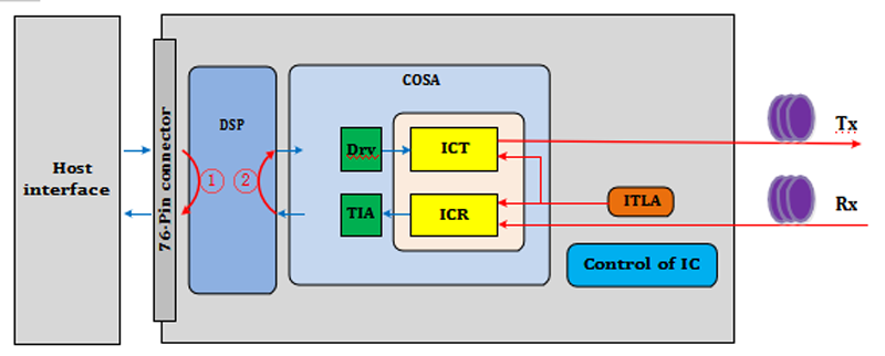
Figure3:Module Loopback Orientation
Optical Specifications
All specifications given in this document are End-of-Life numbers and are valid under operating conditions unless specific noted:
Optical Transmitter Specifications
Parameter | Min | Typ. | Max | Unit | Notes |
Transmitter Frequency Range | 191.3 | 193.7 | 196.1 | THz | C band 75GHz ITU-T grid. Frequency range over which the specifications hold unless noted otherwise. |
Laser Frequency Stability | -1.8 |
| 1.8 | GHz | Frequency stability relative to ITU grid. |
Laser Frequency Accuracy | -1.8 |
| 1.8 | GHz |
|
Laser Frequency Fine Tuning Range | -6.0 |
| 6.0 | GHz |
|
Fine Tuning Resolution |
| 100 |
| MHz |
|
Channel Tuning Speed | - |
| 60 | s |
|
Laser Line Width |
|
| 100 | kHz |
|
Transmitter Output Power Range |
| -9.5 |
| dBm |
|
Transmitter Laser Disable Time |
|
| 180 | ms |
|
Output Power Stability | -0.5 |
| 0.5 | dB | Difference over temperature, time, wavelength and aging. |
Output Power Accuracy | -2 |
| 2 | dB | Difference between the set value and actual value over aging. |
Transmitter Turn-up Time from Cold Start | - |
| 120 | s |
|
Transmitter OSNR (Inband) | 34 |
| - | dB/0.1nm |
|
Transmitter Back Reflectance | - |
| -24 | dB |
|
Transmitter Output Power with TX Disabled | - |
| -20 | dBm |
|
Transmitter Polarization Dependent Power | - |
| 1.5 | dB | Power deference between X and Y polarization |
Optical Receiver Specifications
Parameter | Min | Typ. | Max | Unit | Notes |
Receiver Frequency Range | 191.3 | 193.7 | 196.1 | THz |
|
Input Power Range | -12 |
| 0 | dBm | Signal power of the channel at the OSNR Penalty < 0.5dB |
OSNR Sensitivity |
| 24 | 26 | dB/0.1nm |
|
Receiver Sensitivity |
|
| -20 | dBm | Input power needed to achieve post FEC BER < 1E-15 when OSNR Tolerance > 26dB/0.1nm |
Los Assert | -24 |
| -20 | dBm |
|
Los Hysteresis | 1.0 |
| 2.5 | dB |
|
CD Tolerance | 2400 |
|
| ps/nm | Tolerance to Chromatic Dispersion. |
PMD Tolerance | 10 |
|
| ps | Tolerance to PMD with < 0.5 dB penalty to OSNR sensitivity. |
Peak PDL Tolerance | 3.5 |
|
| dB | Tolerance to peak PDL with < 1.3 dB penalty to OSNR sensitivity when change in SOP is < =1 rad/ms. |
Tolerance to Change in SOP | 50 |
| - | rad/ms |
|
Input Power Transient Tolerance | -2 |
| 2 | dB | Tolerance to change in input power with <0.5 dB penalty to OSNR sensitivity. |
Input Power Reading Accuracy | -2 |
| 2 | dB |
|
Optical Return Loss | -20 |
|
| dB | Optical reflectance at Rx connector input. |
Receiver Turn-up Time from Cold Start | - |
| 120 | s | From module reset, with valid optical input signal present. |
Insertion, Extraction and Retention Force
Parameter | Min | Max | Unit | Note |
Insertion Force |
| 90 | N |
|
Extraction Force |
| 50 | N |
|
Retention Force | 90 |
| N |
|
EMI, EMC and ESD Specification
The module is compliant with the requirements listed in the table below when installed in the host equipment.
Parameter | Reference | Value | Unit | Notes |
ESD Immunity | IEC 61000-4-2 | 8 | kV | Contact Disge |
15 | kV | Air Disge |
ESD (HBM model) | JEDEC JESD22-A114-B | 1 | kV | High-Speed Contacts |
2 | kV | Other pins |
EMC Immunity | IEC 61000-4-3 |
|
|
|
EMI Emission | FCC Class B |
|
|
|
Outline Drawing (mm)

Figure4:QSFP-DD Module Mechanical drawing
 Internet Data Center
 FAQs
FAQs Industry News
 About Us
 Data Center Switch
  Enterprise Switch
  Industrial Switch
  Access Switch
  Integrated Network
  Optical Module & Cable




 Call us on:
  Email Us:
  Room 2106, 3D Building, Tianan Yungu Industrial Park, Xuegang Road No.2018, Bantian, Longgang, Shenzhen, P.R.C.