The tunable 10 Gb/s XFP transceiver is an integrated fiber optic transceiver that provides a high-speed serial link at signaling rates from 9.95 Gb/s to 11.35 Gb/s. The module complies with the 10 Gigabit small form factor pluggable (XFP) multisource agreement-MSA (INF-8077i) and Tunable XFP for ITU Frequency Grid Applications(SFF-8477).
It complies with the ITU-T G.698.1 standard with 50 GHz channel spacing for SONET/SDH, IEEE DWDM 10GBASE-ZR for 80 km reach (Ethernet), and DWDM 10GFC for 80 km reach (Fiber Channel) applications.
The transceiver integrates the receiver and transmit path on one module. On the transmit side, the 10 Gbps serial data stream is recovered, retimed, and passed to a modulator driver. The modulator driver biases and modulates a C-band-tunable integrated laser Mach-Zehnder (ILMZ), enabling data transmission over single-mode fiber through an industry-standard LC connector. On the receiver side, the 10 Gbps data stream is recovered from an APD/ trans-impedance amplifier, retimed, and passed to an output driver. This module features a hot-pluggable XFI-compliant electrical interface.
Features
● Supports 9.95Gb/s to 11.3Gb/s bit rates
● Monolithically integrated full C-band tunable transmitter
● 50 GHz ITU channel spacing with integrated wavelength locker
● C-band-tunable Laser and APD receiver
● Maximum link length of 80km
● Full Duplex LC connector
● Hot-pluggable XFP footprint
● Supports Line-side and XFI loopback
● No Reference Clock required
● Built-in digital diagnostic functions
● Standard bail release mechanism
● Power dissipation <3.5W
● Case temperature range:0°C to 70°C
LA-OT-10GTDW-X80 Wavelength Guide Pin Descriptions
Channel | Wavelength(nm) | Frequency (THZ) | Channel | Wavelength (nm) | Frequency (THZ) |
|
|
| 44 | 1546.12 | 193.9 |
1 | 1563.45 | 191.75 | 45 | 1545.72 | 193.95 |
2 | 1563.05 | 191.8 | 46 | 1545.32 | 194 |
3 | 1562.64 | 191.85 | 47 | 1544.92 | 194.05 |
4 | 1562.23 | 191.9 | 48 | 1544.53 | 194.1 |
5 | 1561.83 | 191.95 | 49 | 1544.13 | 194.15 |
6 | 1561.42 | 192 | 50 | 1543.73 | 194.2 |
7 | 1561.01 | 192.05 | 51 | 1543.33 | 194.25 |
8 | 1560.61 | 192.1 | 52 | 1542.94 | 194.3 |
9 | 1560.2 | 192.15 | 53 | 1542.54 | 194.35 |
10 | 1559.79 | 192.2 | 54 | 1542.14 | 194.4 |
11 | 1559.39 | 192.25 | 55 | 1541.75 | 194.45 |
12 | 1558.98 | 192.3 | 56 | 1541.35 | 194.5 |
13 | 1558.58 | 192.35 | 57 | 1540.95 | 194.55 |
14 | 1558.17 | 192.4 | 58 | 1540.56 | 194.6 |
15 | 1557.77 | 192.45 | 59 | 1540.16 | 194.65 |
16 | 1557.36 | 192.5 | 60 | 1539.77 | 194.7 |
17 | 1556.96 | 192.55 | 61 | 1539.37 | 194.75 |
18 | 1556.55 | 192.6 | 62 | 1538.98 | 194.8 |
19 | 1556.15 | 192.65 | 63 | 1538.58 | 194.85 |
20 | 1555.75 | 192.7 | 64 | 1538.19 | 194.9 |
21 | 1555.34 | 192.75 | 65 | 1537.79 | 194.95 |
22 | 1554.94 | 192.8 | 66 | 1537.4 | 195 |
23 | 1554.54 | 192.85 | 67 | 1537 | 195.05 |
24 | 1554.13 | 192.9 | 68 | 1536.61 | 195.1 |
25 | 1553.73 | 192.95 | 69 | 1536.22 | 195.15 |
26 | 1553.33 | 193 | 70 | 1535.82 | 195.2 |
27 | 1552.93 | 193.05 | 71 | 1535.43 | 195.25 |
28 | 1552.52 | 193.1 | 72 | 1535.04 | 195.3 |
29 | 1552.12 | 193.15 | 73 | 1534.64 | 195.35 |
30 | 1551.72 | 193.2 | 74 | 1534.25 | 195.4 |
31 | 1551.32 | 193.25 | 75 | 1533.86 | 195.45 |
32 | 1550.92 | 193.3 | 76 | 1533.47 | 195.5 |
33 | 1550.52 | 193.35 | 77 | 1533.07 | 195.55 |
34 | 1550.12 | 193.4 | 78 | 1532.68 | 195.6 |
35 | 1549.72 | 193.45 | 79 | 1532.29 | 195.65 |
36 | 1549.32 | 193.5 | 80 | 1531.9 | 195.7 |
37 | 1548.91 | 193.55 | 81 | 1531.51 | 195.75 |
38 | 1548.51 | 193.6 | 82 | 1531.12 | 195.8 |
39 | 1548.11 | 193.65 | 83 | 1530.72 | 195.85 |
40 | 1547.72 | 193.7 | 84 | 1530.33 | 195.9 |
41 | 1547.32 | 193.75 | 85 | 1529.94 | 195.95 |
42 | 1546.92 | 193.8 | 86 | 1529.55 | 196 |
43 | 1546.52 | 193.85 | 87 | 1529.16 | 196.05 |
Non-ITU | Peak wavelength between 1528.77nm-1563.45nm | 88 | 1528.77 | 196.1 |
Note:
1. When a tunable module is plugged in for the first time, it will go to a default channel, or Tx_DIS asserted it will go to a standby condition. LA-OT-10GTDW-X80 default channel is 1563.45nm, compatible with channel range from 1 to 88.
2. When the module is power cycled it will automatically go to the last channel ed, or Tx_DIS asserted it will go to a standby condition. If Tx_DIS asserted, the last channel ed will be cleared, and a valid new channel command will be required to set a channel.
3. If the Tx disabled and then re-enabled, the module returns to the last channel ed.
Absolute Maximum Ratings
Parameter | Symbol | Min | Typ | Max | Unit | Note |
Maximum Supply Voltage 1 | Vcc3 | -0.5 |
| 4.0 | V |
|
Maximum Supply Voltage 2 | Vcc5 | -0.5 |
| 6.0 | V |
|
Storage Temperature | TS | -40 |
| 85 | °C |
|
Case Operating Temperature | Tcase | 0 |
| 70 | °C |
|
Electrical Characteristics
Parameter | Symbol | Min | Typ | Max | Unit | Note |
Main Supply Voltage | Vcc5 | 4.75 |
| 5.25 | V |
|
Supply Voltage #2 | Vcc3 | 3.13 |
| 3.45 | V |
|
Supply Current – Vcc5 supply | Icc5 |
|
| 350 | mA |
|
Supply Current – Vcc3 supply | Icc3 |
|
| 450 | mA |
|
Module total power | P |
|
| 3.5 | W | 1 |
Transmitter |
Input differential impedance | Rin |
| 100 |
| Ω | 2 |
Differential data input swing | Vin,pp | 120 |
| 820 | mV |
|
Transmit Disable Voltage | VD | 2.0 |
| Vcc | V |
|
Transmit Enable Voltage | VEN | GND |
| GND+ 0.8 | V |
|
Receiver |
Differential data output swing | Vout,pp | 340 | 650 | 850 | mV | 3 |
LOS Fault | VLOS fault | Vcc – 0.5 |
| VccHOST | V | 4 |
LOS Normal | VLOS norm | GND |
| GND+0.5 | V | 4 |
Notes:
1. Maximum total power value is specified across the full temperature and voltage range.
2. After internal AC coupling.
3. Into 100 ohms differential termination.
4. Loss Of Signal is open collector to be pulled up with a 4.7k – 10kohm resistor to 3.15 – 3.6V. Logic 0 indicates normal operation; logic 1 indicates no signal detected.
Optical Characteristics
Parameter | Symbol | Min | Typ | Max | Unit | Note |
Transmitter |
Average Optical Power | Pf | -1 |
| 3 | dBm |
|
Wavelength range |
| 1528.77 |
| 1563.45 | nm | LA-OT-10GTDW-X80 |
Optical Wavelength | λc | λc -0.05 |
| λc+0.05 | nm |
|
Center Wavelength Spacing |
|
| 50 |
| GHz | 1 |
Frequency stability (BOL) |
| -1.5 |
| 1.5 | GHz |
|
Frequency stability (EOL) |
| -2.5 |
| 2.5 | GHz |
|
Side mode Suppression ratio | SMSR | 30 |
|
| dB |
|
Optical Extinction Ratio | ER | 9 |
|
| dB |
|
Transmitter and Dispersion Penalty | TDP |
|
| 3 | dB |
|
Average Launch power of OFF transmitter | POFF |
|
| -30 | dBm |
|
Receiver |
Rx Sensitivity | RSENS |
|
| -24 | dBm | Back-to-back ,2 |
|
| -21.5 |
| Fiber (-300 to 1450ps/nm) |
Input Saturation Power (Overload) | Psat | -7 |
|
| dBm |
|
Wavelength Range | λC | 1260 |
| 1600 | nm |
|
Receiver Reflectance | Rrx |
|
| -27 | dB |
|
LOS De-Assert | LOSD |
|
| -27 | dBm |
|
LOS Assert | LOSA | -37 |
|
| dBm |
|
LOS Hysteresis |
| 0.5 |
|
| dB |
|
Notes:
1. Corresponds to approximately 0.4 nm.
2. Measured with worst ER; BER<10-12 with 10.3Gbps,231 – 1 PRBS.
Pin Assignment
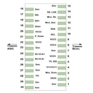
Diagram of Host Board Connector Block Pin Numbers and Name
Pin | Logic | Symbol | Name/Description | Note |
1 |
| GND | Module Ground | 1 |
2 |
| VEE5 | Optional –5.2 Power Supply – Not required |
|
3 | LVTTL-I | Mod-Desel | Module De-; When held low allows the module to respond to 2-wire serial interface commands |
|
4 | LVTTL-O | Interrupt | Interrupt (bar); Indicates presence of an important condition which can be read over the serial 2-wire interface | 2 |
5 | LVTTL-I | TX_DIS | Transmitter Disable; Transmitter laser source turned off |
|
6 |
| VCC5 | +5 Power Supply |
|
7 |
| GND | Module Ground | 1 |
8 |
| VCC3 | +3.3V Power Supply |
|
9 |
| VCC3 | +3.3V Power Supply |
|
10 | LVTTL-I | SCL | Serial 2-wire interface clock | 2 |
11 | LVTTLI/O | SDA | Serial 2-wire interface data line | 2 |
12 | LVTTL-O | Mod_Abs | Module Absent; Indicates module is not present. Grounded in the module. | 2 |
13 | LVTTL-O | Mod_NR | Module Not Ready; Lanbras defines it as a logical OR between RX_LOS and Loss of Lock in TX/RX. | 2 |
14 | LVTTL-O | RX_LOS | Receiver Loss of Signal indicator | 2 |
15 |
| GND | Module Ground | 1 |
16 |
| GND | Module Ground | 1 |
17 | CML-O | RD- | Receiver inverted data output |
|
18 | CML-O | RD+ | Receiver non-inverted data output |
|
19 |
| GND | Module Ground | 1 |
20 |
| VCC2 | +1.8V Power Supply – Not required |
|
21 | LVTTL-I | P_Down/RST | Power Down; When high, places the module in the low power stand-by mode and on the falling edge of P_Down initiates a module reset |
|
|
|
| Reset; The falling edge initiates a complete reset of the module including the 2-wire serial interface, equivalent to a power cycle. |
|
22 |
| VCC2 | +1.8V Power Supply – Not required |
|
23 |
| GND | Module Ground | 1 |
24 | PECL-I | RefCLK+ | Reference Clock non-inverted input, AC coupled on the host board – Not required | 3 |
25 | PECL-I | RefCLK- | Reference Clock inverted input, AC coupled on the host board – Not required | 3 |
26 |
| GND | Module Ground | 1 |
27 |
| GND | Module Ground | 1 |
28 | CML-I | TD- | Transmitter inverted data input |
|
29 | CML-I | TD+ | Transmitter non-inverted data input |
|
30 |
| GND | Module Ground | 1 |
Notes:
1. Module circuit ground is isolated from module chassis ground within the module.
2. 2 Open collector; should be pulled up with 4.7k – 10kohms on host board to a voltage between 3.15V and 3.6V.
3. A Reference Clock input is not required by the XFP 80km tunable. If present, it will be ignored.
Digital Diagnostic Functions
XFP 80km tunable transceivers provide digital diagnostic functions via a 2-wire serial interface, which allows real-time access to the following operating parameters:
• Transceiver temperature
• Laser bias current
• Transmitted optical power
• Received optical power
• Transceiver supply voltage
It also provides a sophisticated system of alarm and warning flags, which may be used to end-users when particular operating parameters are outside of a factory-set normal range.
The operating and diagnostics information is monitored and reported by a Digital Diagnostics Transceiver Controller inside the transceiver, which is accessed through the 2-wire serial interface. When the serial protocol is activated, the serial clock signal (SCL pin) is generated by the host. The positive edge clocks data into the XFP transceiver into those segments of its memory map that are not write-protected. The negative edge clocks data from the XFP transceiver. The serial data signal (SDA pin) is bi-directional for serial data transfer. The host uses SDA in conjunction with SCL to mark the start and end of serial protocol activation. The memories are organized as a series of 8-bit data words that can be addressed individually or sequentially. The 2-wire serial interface provides sequential or random access to the 8-bit parameters, addressed from 000h to the maximum address of the memory.
For more detailed information including memory map definitions, please see the XFP Specification.
Outline Drawing (mm)

Application
● DWDM 10GBASE-ZR/ZW 10G Ethernet
● DWDM 80KM 10G Fiber Channel
● DWDM SONET OC-192&SDH STM-64
 Internet Data Center
 FAQ
FAQ Company News
 About Us
 Data Center Switch
  Enterprise Switch
  Industrial Switch
  Access Switch
  Integrated Network
  Optical Module & Cable





 Call us on:
  Email Us:
  Room 2106, 3D Building, Tianan Yungu Industrial Park, Xuegang Road No.2018, Bantian, Longgang, Shenzhen, P.R.C.